


 +86-731-89578196
 [email protected]

- Home
- Our Company
-
Products
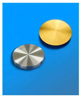
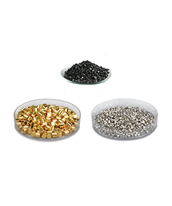
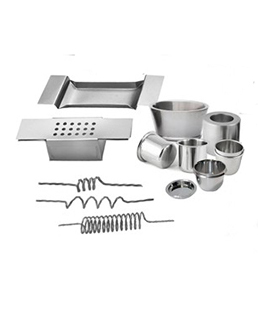
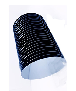
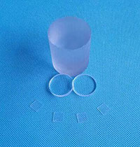
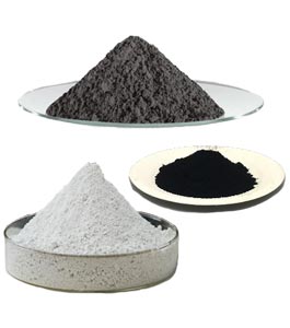
Sputtering Targets
- Industries
- Blog
- FAQ
- Contact Us
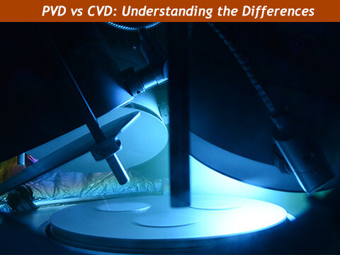
PVD vs CVD: Differences in Thin Film Deposition Techniques
Thin film deposition techniques are crucial for depositing thin films onto a substrate, and the most commonly used methods are physical vapor deposition (PVD) and chemical vapor deposition (CVD).
However, PVD and CVD differ in their processes, applications, and advantages, meaning it's important to understand the differences between them. This article aims to explain the fundamental principles of PVD and CVD, compare their advantages and disadvantages, and examine their applications in various industries.
Whether you're new to thin film deposition or an experienced professional, this article will provide valuable insights to help you make informed decisions and achieve the best results in your projects. So, let's explore the world of PVD and CVD and discover their unique features and capabilities.
What is PVD?
In the field of thin film deposition, Physical Vapor Deposition (PVD) is a popular technique that involves vaporizing a solid material in a vacuum chamber. The process begins with heating a solid material, like metal or alloy, which causes it to vaporize and form a plasma of ions and neutral particles.
This plasma is then directed towards a substrate made of glass, metal, or semiconductor material, where the ions and particles in the plasma condense and form a thin film. The thickness of the film can be controlled by adjusting the deposition time and the rate of material vaporization.
PVD is a versatile technique that can be used to deposit thin films of various materials, including metals, alloys, and ceramics. It can also be used to create multilayered thin films by sequentially depositing different materials to form a complex structure.
Compared to other thin film deposition techniques, PVD has several advantages, such as high purity, uniformity, and adhesion. It is widely used in industries such as semiconductor, optical, and automotive, where high-quality thin films are crucial for product performance and reliability.
What is CVD?
Thin films can be deposited using a technique called Chemical Vapor Deposition (CVD). This process involves introducing a gas or vapor into a vacuum chamber containing a substrate. Through a thermal or plasma-assisted process, the gas or vapor reacts with the substrate to form a solid thin film. The thickness of the film can be regulated by varying the deposition time and the concentration of the gas or vapor.
CVD is a versatile technique that can deposit thin films of various materials like metals, semiconductors, and ceramics. It can also create complex structures, such as nanowires and nanotubes. Compared to other deposition techniques, CVD has several benefits, including high purity, uniformity, and conformality. It is widely used in industries such as semiconductor, aerospace, and biomedical where the properties of the thin film are critical for performance and reliability.
Differences between PVD and CVD
PVD and CVD have different processes, applications, and benefits. The key contrast between PVD and CVD lies in how the thin film is placed on the substrate. PVD involves vaporizing the solid material and condensing it onto the substrate, whereas CVD involves the gas or vapor reacting with the substrate to create a solid thin film. This fundamental distinction results in numerous other variations between the two methods.
Process Complexity
The process of PVD involves vaporizing a solid material and then condensing it onto a substrate. This can be controlled by changing the deposition time, the rate of material vaporization, and the substrate temperature.
On the other hand, CVD is a more intricate process that involves a reaction between gas or vapor and the substrate. This can be controlled by adjusting the concentration of the gas or vapor, the substrate temperature, and the pressure in the vacuum chamber.
Film Quality
When it comes to producing high-quality thin films, PVD and CVD have different strengths. PVD is renowned for its ability to create pure, uniform, and adhesive films, making it ideal for applications that require precise control over thin film properties.
CVD, on the other hand, is highly conformal, allowing it to coat complex geometries and structures. However, CVD can be prone to impurities and defects in the thin film, which can impact its properties and performance.
Material Compatibility
PVD is best for depositing thin films of metals, alloys, and ceramics, whereas CVD is better suited for depositing thin films of metals, semiconductors, and ceramics. The selection of the process depends on the qualities of the material, the desired properties of the thin film, and the needs of the particular application.
PVD vs CVD: Which is the better option?
The choice between PVD and CVD depends on several factors, such as:
Material properties
The technique chosen depends on the properties of the materials, including their melting and boiling points, as well as their reactivity. PVD is best for materials with high melting points and low reactivity, while CVD is more appropriate for materials with low melting points and high reactivity.
Thin film properties
The technique chosen for creating a thin film depends on the specific properties desired, including thickness, composition, and crystallinity. PVD is best suited for applications requiring high purity, uniformity, and adhesion, while CVD is better for applications that require precise control over thin film properties and conformality.
Application requirements
When choosing a technique, it's important to consider the application requirements, such as substrate geometry, deposition rate, and deposition temperature. PVD works well for flat substrates with high deposition rates, while CVD is better suited for irregular substrates with low deposition rates.
Conclusion
To summarize, PVD and CVD are two frequently utilized methods for depositing thin films, each with its own distinct qualities and abilities. Although both techniques are used for the same purpose, they differ in terms of their processes, uses, and benefits.
It is essential for researchers, engineers, and manufacturers to comprehend the differences between the two methods in order to select the appropriate technique for their particular needs.
By taking into account the material characteristics, the desired thin film features, and the application requirements, informed decisions can be made and optimal outcomes can be achieved in their projects.
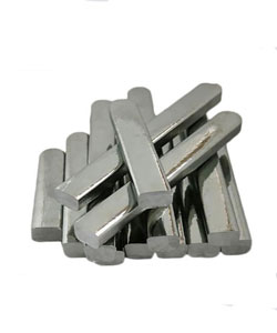
If you want to know more about Sputtering Target Used in PVD and CVD, you can contact our raw material expert.