


 +86-731-89578196
 [email protected]

- Home
- Our Company
-
Products
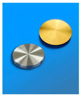
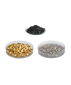
Sputtering Targets
- Industries
- Blog
- FAQ
- Contact Us


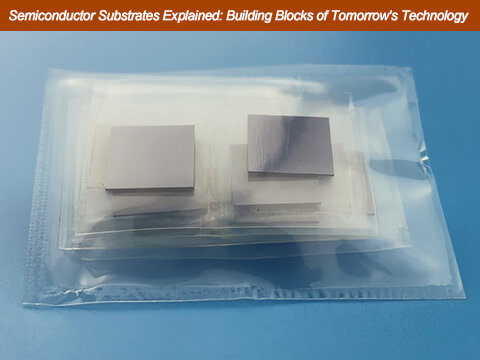
Semiconductor Substrates Explained: Building Blocks of Tomorrow's Technology
Introduction to Semiconductor Substrates
Semiconductor substrates are essential materials in modern electronics. They serve as the foundation for various semiconductor devices. These substrates provide the physical platform on which circuits and electronic components are built. Without them, the complex circuits found in devices like computers, smartphones, and other technologies wouldn't function. The role of semiconductor substrates goes beyond just being a base material. They also impact the overall performance, efficiency, and reliability of the devices.
In the world of semiconductors, substrates are more than just a starting point for electronics. They influence power consumption, speed, heat dissipation, and the miniaturization of electronic components. As technology advances, the demand for high-quality and advanced substrates grows. This makes them crucial for industries like telecommunications, automotive, aerospace, and consumer electronics.
What Are Semiconductor Substrates?
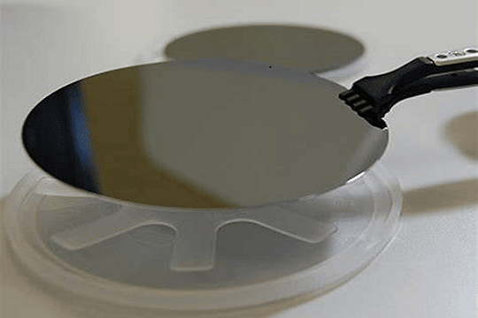
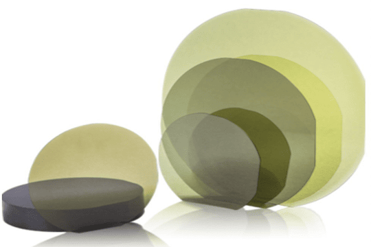
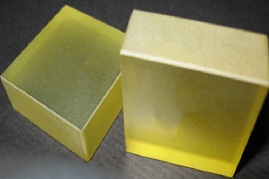
A semiconductor substrate is typically a wafer made from materials that have unique electrical properties, such as silicon, gallium arsenide (GaAs), or silicon carbide (SiC). These materials are semiconductors, meaning they can conduct electricity under certain conditions. This makes them ideal for creating devices like transistors, diodes, and integrated circuits.
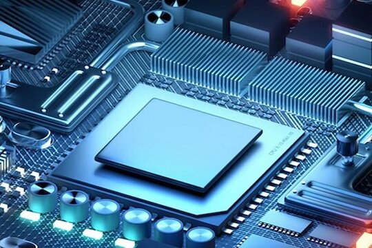
In a typical semiconductor device, the substrate acts as the foundation upon which additional layers are built. During the manufacturing process, thin layers of materials are deposited onto the substrate, and microscopic circuits are etched into these layers. These circuits are what enable the device to perform tasks like computing, data storage, and communication.
The importance of semiconductor substrates lies in their ability to control the flow of electricity. The choice of substrate material determines how well the device will perform under specific conditions, such as high temperatures or high voltages. For example, silicon is used for most consumer electronics because it is abundant and has excellent electrical properties. However, for high-power or high-frequency applications, materials like gallium arsenide or silicon carbide are preferred because they offer better performance in extreme conditions.
Types of Semiconductor Substrates
1. Silicon Substrates
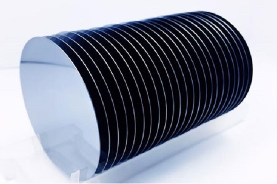
Silicon is by far the most common material used in the production of semiconductor devices. Silicon wafers are thin slices of silicon crystals that serve as the base for manufacturing integrated circuits (ICs). Silicon’s popularity stems from its abundance in nature and its excellent semiconductor properties. It can conduct electricity when doped with other elements, such as phosphorus or boron, allowing it to be used in a wide range of electronic applications.
Silicon wafers are the backbone of the semiconductor industry. They are used in the production of everything from microprocessors to memory chips, and their relatively low cost and easy availability make them an ideal choice for most electronic devices. Additionally, silicon is highly versatile — it can be used to manufacture both digital and analog circuits, making it the material of choice for the majority of electronics.
2. Single-Crystal Silicon
Single-crystal silicon is the most widely used semiconductor substrate material. Its uniform structure, free from defects, makes it ideal for producing high-performance electronic devices. This material's excellent electrical properties and stability allow for seamless integration into microchips, transistors, and integrated circuits, forming the backbone of many modern technologies.
3. Gallium Arsenide (GaAs)
Gallium Arsenide is known for its high electron mobility, which makes it suitable for high-speed electronic devices. It performs better than silicon in terms of electron movement, making it the substrate of choice for microwave and high-frequency applications like mobile communication and radar systems. Additionally, GaAs is used in advanced solar cells due to its efficiency in converting light to electrical energy.
4. Silicon Carbide (SiC)
Silicon carbide is gaining popularity in high-power and high-temperature applications, such as power electronics and high-frequency devices. Its excellent thermal conductivity and ability to withstand high voltages make SiC ideal for energy-efficient power systems. It’s also commonly used in LED lighting technology.
5. Sapphire (Al₂O₃)

Sapphire substrates, made from a compound of aluminum and oxygen, are valued for their hardness and durability. They are used in harsh environments and optoelectronic devices, like LEDs. Sapphire also has good thermal conductivity, which helps in dissipating heat from electronic components, preventing overheating.
6. Indium Phosphide (InP)
Indium phosphide is widely used in high-speed and optoelectronic devices, including lasers, transistors, and LEDs. Its high electron mobility makes it ideal for high-frequency applications, while its transparency to certain wavelengths of light supports advanced optical technologies, including fiber optics.
7. Silicon Germanium (SiGe)
Silicon-germanium is a composite material that combines the strengths of both silicon and germanium. It has higher electron mobility than silicon, making it suitable for high-speed transistors in telecommunication and wireless applications. SiGe is often used in processors and RF devices for its ability to improve performance at a relatively lower cost.
8. Germanium (Ge)
Germanium was widely used in early semiconductor devices but has largely been replaced by silicon. However, it remains relevant in specific applications such as infrared detectors and high-efficiency solar cells. Germanium has unique properties that allow for superior sensitivity to light and thermal properties, which are beneficial for niche technologies.
9. Zinc Oxide (ZnO)
Zinc oxide is being researched as an emerging material for semiconductor substrates, especially for its thermal conductivity and optical properties. It has potential in applications like LEDs, UV detectors, and high-temperature electronics due to its ability to withstand extreme conditions.
10. Single-Crystal Aluminum Oxide (Al₂O₃)
Single-crystal aluminum oxide, similar to sapphire, is noted for its hardness and transparency to specific light wavelengths. While it shares many characteristics with sapphire, it’s less widely used in the industry due to higher costs and limited availability. Still, it has niche applications in optical and optoelectronic devices.
How Are Semiconductor Substrates Made?
The process of manufacturing semiconductor substrates is complex. It involves multiple steps to ensure the highest quality and performance.
1. Crystal Growth
The first step in producing semiconductor substrates is growing a large, single crystal of the material. For silicon, this is done using the Czochralski process. In this process, high-purity silicon is melted and a small seed crystal is slowly pulled from the molten material, forming a large cylindrical crystal known as a boule.
2. Wafer Slicing
Once the crystal boule is grown, it is sliced into thin wafers using a diamond-tipped saw. These wafers are typically only a few hundred microns thick. However, they must be perfectly flat and uniform to ensure that the circuits built on them are accurate.
3. Polishing and Cleaning
After slicing, the wafers are polished to achieve a smooth, mirror-like surface. Any imperfections on the surface of the wafer could interfere with the performance of the final device. The wafers are then cleaned to remove any particles or contaminants that could affect the manufacturing process.
4. Quality Control
Quality control is critical in the production of semiconductor substrates. Each wafer undergoes rigorous testing to ensure that it meets the required specifications. This includes checking for defects, measuring thickness, and testing electrical properties.
Why Are Semiconductor Substrates So Important?
Semiconductor substrates play a critical role in determining the performance and reliability of electronic devices. The choice of substrate material can have a significant impact on the device's electrical properties, heat management, and overall durability.
For example, silicon substrates are ideal for most consumer electronics because they offer a good balance of performance and cost. However, for high-performance applications like power electronics or high-frequency communications, materials like silicon carbide or gallium arsenide may be more appropriate due to their superior electrical and thermal properties.
Applications of Semiconductor Substrates
Semiconductor substrates are used in a wide range of electronic devices, from everyday consumer products to advanced industrial systems.
1. Microprocessors and Memory Chips
Microprocessors, the brains of computers and smartphones, rely on silicon substrates to function efficiently. Memory chips, which store data, also use silicon wafers as their base material.
2. Power Electronics

Silicon carbide substrates are increasingly being used in power electronics, such as electric vehicles and solar power systems. SiC's ability to handle high voltages and temperatures makes it ideal for these applications.
3. 5G Networks

Gallium arsenide substrates are widely used in telecommunications, particularly in 5G networks. GaAs substrates enable devices to operate at higher frequencies, allowing for faster data transmission.
Future Trends in Semiconductor Substrates
As technology evolves, so do the requirements for semiconductor substrates. Researchers are exploring new materials like graphene and new manufacturing techniques to improve the performance and efficiency of electronic devices. One of the most exciting developments is the move toward 3D integrated circuits, where multiple layers of electronic components are stacked on top of each other, allowing for more powerful and compact devices.
Conclusion
Semiconductor substrates may not be visible in the final product, but they are crucial to the operation of modern electronics. These materials are the foundation of the devices that power our world, from smartphones to electric cars to 5G networks. As technology continues to advance, the importance of high-quality semiconductor substrates will only grow, driving innovation and shaping the future of electronics.
If you're looking for reliable, high-quality semiconductor substrates to power your next innovation, we are here to help! With a wide range of advanced materials like silicon, gallium arsenide, and silicon carbide, we can meet your specific project requirements. Contact us today to learn more about our products and how we can assist you in taking your technology to the next level. Our team of experts is ready to provide you with the best solutions for your electronic and semiconductor needs!