


 +86-731-89578196
 [email protected]

- Home
- Our Company
-
Products
Sputtering Targets
- Industries
- Blog
- FAQ
- Contact Us
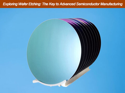
Exploring Wafer Etching: The Key to Advanced Semiconductor Manufacturing
Wafer etching is a crucial step in semiconductor manufacturing. It allows the creation of detailed patterns on silicon wafers. These patterns are essential for making integrated circuits and various semiconductor devices. In this blog, we will explore the types of wafer etching, the etching process, applications, advantages, challenges, and future trends in the industry.
Introduction to Wafer Etching
Wafer etching involves removing layers from a wafer’s surface to form precise patterns needed for electronic circuits. This process is vital in the semiconductor industry. It enables the miniaturization and performance improvements of electronic devices. By understanding wafer etching, we can appreciate its critical role in modern technology.
Types of Wafer Etching Techniques
Dry Etching
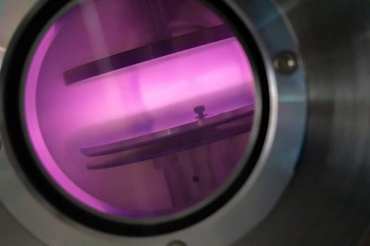
Dry etching is a process that uses gases and plasmas to remove material from the wafer. This type of etching is known for its precision and ability to create intricate and well-defined patterns. There are several techniques within dry etching. Each has its own specific applications and benefits.
Plasma Etching
Plasma etching is a widely used dry etching technique that involves the use of plasma, a highly energized state of matter. Plasma is created by applying a high-frequency voltage to a gas, which ionizes the gas and creates reactive ions and radicals. These reactive species interact with the wafer material, etching it away. Plasma etching is particularly effective for fine features and can be controlled with high precision.
- How It Works: Plasma etching uses a combination of physical and chemical processes. The physical process involves the bombardment of the wafer surface by ions, which helps to break bonds in the material. The chemical process involves the reaction of reactive species with the wafer material. This can form volatile by-products that can be removed.
- Applications: Plasma etching is commonly used for patterning dielectric materials, such as silicon dioxide and silicon nitride. It can also be used for etching metals and other semiconductor materials.
Reactive Ion Etching (RIE)
Reactive ion etching (RIE) is a dry etching technique that combines the principles of plasma etching with ion bombardment. In RIE, the wafer is placed in a chamber where a plasma is generated, and ions from the plasma are accelerated towards the wafer surface. This ion bombardment enhances the etching process. And it allows for more precise control over the etching profile.
- How It Works: RIE uses a combination of physical and chemical etching. The physical aspect involves the acceleration of ions towards the wafer surface, which helps to remove material. The chemical aspect involves the reaction of reactive species with the wafer material to form volatile by-products.
- Advantages: RIE is known for its ability to create anisotropic etching profiles. This means that the etch rate is different in different directions. This is crucial for creating vertical sidewalls in microstructures.
- Applications: RIE is widely used in the fabrication of integrated circuits, MEMS devices. It's also used in other semiconductor components that require precise patterning.
Deep Reactive Ion Etching (DRIE)
Deep reactive ion etching (DRIE) is a specialized form of RIE that is used to create deep, high-aspect-ratio features. DRIE alternates between etching and passivation steps. This can achieve deep etches with smooth sidewalls. This technique is particularly important for applications that require deep trenches or high-aspect-ratio structures.
- How It Works: DRIE uses a cyclical process that alternates between etching and passivation. During the etching phase, the wafer is exposed to a plasma that removes material. During the passivation phase, a protective layer is deposited on the sidewalls of the etched features. This can prevent lateral etching. This alternating process allows for the creation of deep, narrow features with vertical sidewalls.
- Advantages: DRIE is capable of creating extremely deep and narrow features with high precision. It is also capable of achieving high aspect ratios. This makes it ideal for applications that require deep trenches or vertical sidewalls.
- Applications: DRIE is widely used in the fabrication of MEMS devices, such as accelerometers and gyroscopes. It's also used in the creation of deep trenches for isolation and interconnects in integrated circuits.
Wet Etching
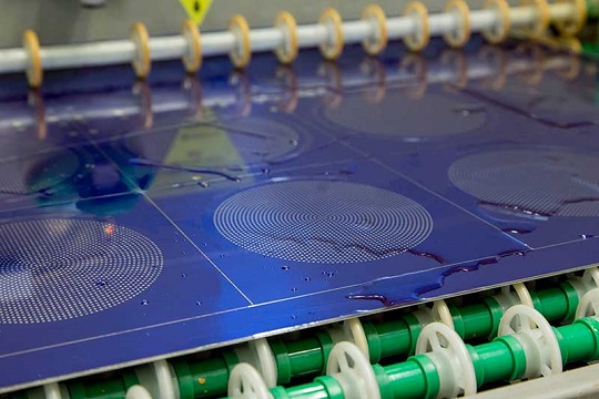
Wet etching is a process that uses liquid chemicals to remove material from the wafer. This type of etching is typically less precise than dry etching. But it's still widely used for certain applications due to its simplicity and effectiveness. Wet etching can be either isotropic or anisotropic. This depends on the chemical solution and the material being etched.
Chemical Etching
Chemical etching is the most common type of wet etching. It involves submerging the wafer in a chemical solution that reacts with the material to be removed. The etch rate can vary depending on the chemical used and the material of the wafer.
- How It Works: Chemical etching relies on the reaction between the etching solution and the wafer material. The solution dissolves the material, forming soluble by-products that can be washed away. The etch rate is influenced by factors such as the concentration of the etching solution, the temperature, and the agitation of the solution.
- Advantages: Chemical etching is relatively simple and cost-effective. It can also etch large areas uniformly, making it suitable for applications that do not require high precision.
- Applications: Chemical etching is commonly used for etching metals, such as aluminum and copper. It's also used for patterning silicon dioxide and other dielectric materials.
Isotropic vs. Anisotropic Etching
- Isotropic Etching: Isotropic etching removes material uniformly in all directions, leading to rounded features. This type of etching is useful for applications where uniform removal is needed, but it can be less precise for creating fine patterns.
- Anisotropic Etching: Anisotropic etching removes material at different rates in different directions. This allows for more precise and defined patterns. This type of etching is essential for applications that require vertical sidewalls and well-defined features.
The Wafer Etching Process
Preparation and Cleaning
Before etching, wafers undergo thorough cleaning. This works to remove any contaminants that might interfere with the etching process. This step is crucial for ensuring that the etching proceeds uniformly and accurately.
Masking
Photolithography: A photoresist, which is a light-sensitive material, is applied to the wafer. Using ultraviolet (UV) light, a pattern is transferred onto the photoresist through a mask. This pattern protects certain areas of the wafer during etching.
Mask Materials: Common materials used for masks include silicon dioxide (SiO2) and silicon nitride (Si3N4). They are both resistant to the etching chemicals and processes used.
Etching
Etching Parameters: Various parameters, such as gas flow rates, RF power, and etch time, are carefully controlled during the etching process to achieve the desired depth and profile of the etched features.
Process Control: Advanced monitoring systems are used to ensure the etching process remains consistent and produces high-quality patterns. These systems can detect deviations and make real-time adjustments.
Post-Etching Cleaning
Removing Residuals: After etching, any remaining photoresist and by-products from the etching process are removed through cleaning steps.
Surface Conditioning: The wafer surface is conditioned to prepare it for subsequent manufacturing steps ensuring it is clean and free from contaminants.
Applications of Wafer Etching
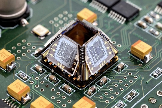
Wafer etching is utilized in various applications across the semiconductor industry:
- Integrated Circuits (ICs): Wafer etching is fundamental for creating the tiny transistors and interconnects that make up microchips.
- Microelectromechanical Systems (MEMS): Used in sensors, actuators, and other devices found in automotive, medical, and consumer electronics.
- Photonic Devices: Essential for creating optical components used in telecommunications and data transfer.
- Other Semiconductor Devices: Including LEDs, solar cells, and more. They benefit from the precision of wafer etching.
Advantages and Challenges of Wafer Etching
Advantages
- Precision and Accuracy: Wafer etching allows for the creation of extremely fine and detailed patterns. This is essential for modern electronic devices.
- Versatility: Can be used with various materials and for different applications. This makes it a highly adaptable process.
Challenges
- Process Complexity: Wafer etching requires precise control of numerous parameters. This makes it a complex process.
- Contamination Control: Even minor contaminants can significantly impact the quality of the etching process.
- Equipment Costs: High-end etching equipment and facilities are expensive. This adds to the overall cost of semiconductor manufacturing.
Future Trends in Wafer Etching
The field of wafer etching is continuously evolving with new advancements:
- New Etching Technologies: Research is ongoing to develop more advanced etching techniques that offer higher precision and efficiency.
- Emerging Materials and Processes: Innovations in materials and etching processes aim to enhance the performance and capabilities of semiconductor devices.
- Industry Innovations: The semiconductor industry continually innovates to meet the growing demand for smaller, faster, and more efficient electronic devices.
Conclusion
Wafer etching is a fundamental process in semiconductor manufacturing. It enables the creation of intricate patterns on silicon wafers. By understanding the different etching techniques, the detailed etching process, and its wide range of applications, we can appreciate the critical role wafer etching plays in advancing technology. The future of wafer etching looks promising with ongoing innovations and developments, ensuring its continued importance in the semiconductor industry.
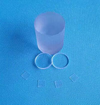
At AEM, we provide high-quality wafers and substrates for various semiconductor applications. We pride ourselves on delivering precision and reliability in every wafer we supply. If you're interested in learning more about our products or placing an order, please contact us. Our team is ready to assist you with all your wafer and substrate needs.