 +86-731-89578196
 [email protected]
- Home
- Our Company
-
Products
Sputtering Targets
- Industries
- Blog
- FAQ
- Contact Us
Wafer Fabrication Guide: Processes, Materials & Trends in 2025
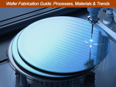
Introduction to Wafer Fabrication
Wafer fabrication is a critical process that powers modern electronics and technology. It's the foundation for creating semiconductors, which are used in everything from smartphones and computers to solar panels and electric vehicles. In this article, we'll break down what wafer fabrication is, why it's so important, and how sourcing wafers from a trusted supplier like AEM Deposition can help your business meet its technology needs.
What is Wafer Fabrication?
Wafer fabrication is the process of creating semiconductor wafers, which are thin, flat discs made from materials like silicon or Gallium. These wafers serve as the base for making integrated circuits (ICs) that power virtually every electronic device. The process itself is highly detailed and involves multiple steps, including slicing raw material, doping, deposition, etching, and testing.
At the start, wafer fabrication begins with a crystal (often silicon) that's grown using a technique called the Czochralski process. This crystal is pulled from molten material, forming a large cylindrical ingot. The ingot is then sliced into thin discs, each one polished to a smooth surface. These polished wafers are then ready for the complex processes that create semiconductor devices, such as microprocessors, memory chips, and sensors.
What is a Semiconductor Wafer?
A semiconductor wafer is a thin, flat disc that serves as the substrate for microelectronic devices like integrated circuits (ICs). Wafers are typically made from silicon, though other materials like Gallium Arsenide (GaAs) and compound semiconductors are also commonly used. These wafers are sliced from large single crystals, which are then processed through various stages to create the structures that will eventually become the components of a microchip.
These wafers provide the foundation for manufacturing semiconductors, and their size, shape, and purity are crucial in determining the final performance of the electronic devices they power.
Types of Wafers: Silicon, Gallium, and More
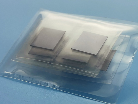
Different types of semiconductor wafers are used in various applications depending on the material properties required. Below are some of the most commonly used wafers in wafer fabrication:
-
Silicon Wafers
Silicon wafers are the most common type of wafer used in the semiconductor industry. Silicon is an ideal material because it is abundant, cost-effective, and has excellent electronic properties. It is widely used in the production of microchips for consumer electronics, computers, and telecommunications equipment. Monocrystalline silicon wafers, with their uniform structure, offer the best performance for high-speed processing and low energy consumption.
-
Gallium Arsenide (GaAs) Wafers
Gallium wafers, particularly Gallium Arsenide (GaAs), are often used in high-frequency and high-power applications, such as radio frequency (RF) components and optical devices. GaAs wafers are preferred for applications where silicon would not perform as well, particularly in optoelectronics, laser diodes, and high-speed telecommunications.
-
Compound Semiconductor Wafers
In addition to silicon and Gallium, other compound semiconductors like Indium Phosphide (InP) and Silicon Carbide (SiC) are also used for specific high-performance applications. These materials are often chosen for their superior thermal conductivity, electrical performance, and ability to withstand higher power levels.
-
Other Specialty Wafers
Wafers made from materials like Germanium (Ge), Sapphire (Al2O3), and Quartz are used in specific niches, such as high-precision sensors, photovoltaic systems, and certain types of LEDs.
Each type of wafer material has its own unique properties that make it suitable for specific applications, and understanding these differences helps businesses select the right wafer for their needs.
Selecting the Right Wafer for Your Business Needs
At AEM Deposition, we understand the importance of these precision steps. Our wafers undergo strict quality control checks at every stage of the process to ensure the highest quality product for our customers. Whether you’re sourcing silicon wafers or Gallium wafers, you can trust that our wafers are produced with cutting-edge technology and stringent standards.
When sourcing wafers for your business, understanding wafer fabrication is key. You’ll want to consider the material, size, and application of the wafer before making your purchase. High-quality wafers can directly impact the performance and efficiency of the products you manufacture, whether it’s consumer electronics, solar panels, or even medical devices.
By choosing a reliable wafer supplier like AEM Deposition, you ensure that your wafers meet your exact specifications and help you create the best possible end products. In the next section, we’ll dive deeper into the process of selecting a wafer supplier and how AEM Deposition stands out as a trusted partner for businesses around the world.
Wafer Fabrication Process Overview
Wafer fabrication is an intricate and multi-step process that requires precise techniques and equipment. From the initial raw material to the final wafer ready for semiconductor device production, each stage is critical to ensure that the wafers meet the required standards for performance and reliability. In this section, we’ll take you through a comprehensive overview of the wafer fabrication process, highlighting the essential steps that are involved in producing high-quality wafers.
Understanding this process is crucial for businesses sourcing wafers, as it can directly impact the quality, efficiency, and functionality of the devices being built. If you are considering sourcing silicon wafers or Gallium wafers, knowing the steps involved in wafer fabrication will help you make an informed decision about the wafers that best meet your business needs.

The wafer fabrication process can be broken down into several core stages. While the steps may vary slightly depending on the type of wafer or the specific requirements of the semiconductor device, they typically follow this general flow:
- Material Preparation
- Wafer Slicing
- Wafer Polishing
- Doping
- Oxidation and Deposition
- Photolithography
- Etching
- Metallization
- Testing and Quality Control
Let’s dive deeper into each of these stages to better understand what happens at each point.
Material Preparation
The fabrication process begins with material preparation, which involves selecting the base material for the wafer. Most wafers are made from silicon, though other materials like Gallium Arsenide (GaAs), Sapphire, and others are also used depending on the application.
- Silicon wafers are generally produced by first growing a single crystal silicon ingot using the Czochralski process. This method involves melting silicon in a crucible and slowly drawing a small silicon seed crystal from the molten silicon, causing the crystal to grow as the ingot is pulled upward. This creates a cylindrical shape, which is later sliced into thin wafers.
- Other materials like Gallium Arsenide or compound semiconductors often follow similar initial preparation techniques but may require additional steps due to their different crystal structures or thermal properties.
Wafer Slicing
After the crystal has grown, the wafer slicing process begins. The silicon ingot is carefully cut into thin slices (wafers) using a diamond wire saw. The thickness of the slices depends on the intended application, with wafers typically ranging from 200mm to 300mm in diameter.
Precision is key during this stage, as any deviation can cause the wafer to crack or become unusable. The slicing process must be highly controlled to ensure that each wafer is of consistent thickness and flatness, setting the foundation for the following steps.
Wafer Polishing
Once sliced, the wafers undergo a polishing process. The goal is to create a smooth, mirror-like surface, free from scratches, pits, and any microscopic imperfections. Even minor defects can negatively affect the wafer’s performance, especially in advanced semiconductor manufacturing.
- During polishing, chemical mechanical planarization (CMP) is typically used to achieve a flat surface. This process involves using a combination of chemical slurry and mechanical pressure to smooth out the wafer.
- The result is a pristine, defect-free wafer that can now be subjected to the more complex processes involved in semiconductor fabrication.
Doping
Doping is the process where impurities are introduced to modify the electrical properties of the silicon wafer. This step is crucial for creating the n-type (negative) and p-type (positive) regions that will form the semiconductor junctions within an integrated circuit (IC).
- Doping is done by introducing elements like phosphorus (for n-type) or boron (for p-type) to the wafer. This is often done through a method known as ion implantation, where ions of the dopant material are accelerated and bombarded onto the wafer surface.
- By controlling the type and concentration of doping materials, manufacturers can precisely tailor the wafer’s electrical properties to meet specific design requirements.
Oxidation and Deposition
After doping, wafers undergo a process called oxidation, where a thin layer of silicon dioxide is grown on the surface of the wafer. This layer serves multiple purposes, including:
- Providing insulation between different layers of circuitry.
- Acting as a protective layer during subsequent processing steps.
- Forming the gate dielectric in transistors.
Deposition is another critical process where thin layers of materials such as metals, oxides, or nitrides are added to the wafer. This is typically done using two main techniques:
- Chemical Vapor Deposition (CVD): In CVD, gases react on the wafer’s surface to form a solid material layer.
- Physical Vapor Deposition (PVD): PVD involves using a vacuum to deposit thin metal films onto the wafer.
These layers play essential roles in the creation of electrical connections and the formation of various devices on the wafer.
Photolithography
Photolithography is one of the most important and complex steps in the wafer fabrication process. It involves transferring a detailed pattern (usually designed for an integrated circuit) onto the surface of the wafer. The process uses light to etch patterns onto a light-sensitive material known as photoresist.
- Step 1: A layer of photoresist is applied to the wafer.
- Step 2: The wafer is then exposed to ultraviolet (UV) light through a mask, which contains the pattern that will form the semiconductor device’s circuit.
- Step 3: After exposure, the photoresist is developed, leaving behind a patterned layer that defines the areas of the wafer where material will be removed or altered in the next steps.
This step is repeated multiple times as the wafer is progressively etched and patterned with intricate designs that form the basis of transistors, diodes, capacitors, and other components.
Etching
Etching is a process used to remove the unprotected parts of the wafer after photolithography, creating the desired pattern. There are two main types of etching:
- Wet etching: Involves the use of liquid chemicals to etch away exposed areas.
- Dry etching: Uses gases or plasmas to etch the wafer surface, allowing for more precise control over the process.
Etching creates the intricate, microscopic patterns needed to form the active components of integrated circuits. It’s often referred to as the "sculpting" phase of semiconductor manufacturing, where the electrical pathways and device structures are defined.
Metallization
Metallization involves adding metallic layers (usually copper or aluminum) onto the wafer to form the interconnections between different components of the integrated circuit. These metal layers allow the flow of electrical current between transistors, resistors, and capacitors, effectively creating a fully functional semiconductor device.
The process of metallization is often followed by chemical vapor deposition (CVD) or physical vapor deposition (PVD) to deposit thin layers of metal that are then patterned through photolithography and etching.
Testing and Quality Control
Once all the layers have been deposited and etched, the wafer undergoes extensive testing and inspection to ensure it meets the required specifications. This stage involves several types of tests:
- Electrical testing: To check for correct operation of the circuits on the wafer.
- Optical inspection: To detect any defects or issues with the physical structure of the wafer.
- Microscopic analysis: To identify any microscopic imperfections or damage.
Any wafers that fail these tests are discarded or reworked to meet the necessary quality standards. At AEM Deposition, we ensure that all our wafers undergo rigorous testing to guarantee they meet the highest performance standards for your applications.
The wafer fabrication process is a complex, high-precision journey that transforms raw materials into the foundation for today’s most advanced technology. From slicing and polishing to doping and etching, each step must be performed with exacting standards to ensure the wafers are of the highest quality. By sourcing wafers from a trusted supplier like AEM Deposition, you can be confident that your wafers will meet the stringent requirements of your business, whether you're in the semiconductor, solar, or electronics industry.
Future Trends in Wafer Fabrication
Wafer fabrication is evolving rapidly, driven by the demands of cutting-edge technologies. As industries like semiconductors, 5G, AI, and quantum computing grow, wafer manufacturers must adapt to new materials, processes, and automation techniques. Here’s a closer look at the key trends shaping the future of wafer fabrication.
1. Smaller and More Efficient Nodes
The industry continues to push towards smaller process nodes, with 3nm and even 2nm nodes on the horizon. This trend is essential to meet the growing demand for faster and more efficient microchips.
Impact:
- Photolithography and EUV will be critical for achieving these small nodes.
- Wafer uniformity and defect-free surfaces will become even more crucial to maintain high performance.
2. New Materials Beyond Silicon
While silicon will remain the backbone, new materials like Gallium Nitride (GaN), Silicon Carbide (SiC), and 2D materials are gaining importance, particularly for power electronics and next-gen devices.
Impact:
- Advanced materials require new fabrication techniques, including specialized crystal growth and etching processes.
- These materials will open the door to more efficient, high-performance devices.
3. AI and Automation in Fabrication
AI and automation are revolutionizing wafer fabrication by improving precision and efficiency. Automated systems and AI-driven tools will help in everything from defect detection to process optimization.
Impact:
- Automation will minimize human error and improve wafer consistency.
- AI will optimize process flows, improving yield and reducing costs.
4. 3D Wafer Stacking and Advanced Packaging
3D stacking is becoming a key trend to create higher-density chips in smaller packages. This technique is essential for high-performance applications where traditional 2D designs no longer suffice.
Impact:
- Wafer thinning and bonding techniques will improve as 3D stacking gains traction.
- New packaging methods like flip-chip bonding will further enhance chip performance.
5. Sustainability in Wafer Fabrication
Environmental concerns are driving the semiconductor industry toward eco-friendly practices. Reducing waste, improving energy efficiency, and recycling materials will be essential to meet both environmental regulations and consumer expectations.
Impact:
- Wafer manufacturers will focus on clean energy and water recycling.
- Sustainable manufacturing practices will reduce the environmental footprint of wafer production.
6. Quantum Computing and Precision Fabrication
Quantum computing is one of the most exciting future trends in wafer fabrication. It requires new materials and extreme precision in manufacturing.
Impact:
- Quantum chip fabrication will demand atomic-level precision in wafer production.
- New materials and fabrication techniques will be crucial for developing viable quantum processors.
The future of wafer fabrication is characterized by advancements in process nodes, materials, automation, and sustainability. These trends will drive wafer manufacturing toward higher precision, efficiency, and performance. AEM Deposition is committed to staying at the forefront of these developments to provide the highest-quality wafers to meet the evolving needs of industries worldwide.
Conclusion
Wafer fabrication is a true testament to human innovation, turning raw materials into the tiny components that power our technology. From the growth of a single crystal to the precise interaction of light and chemicals, this process allows us to manipulate matter at the atomic level.
As technology evolves, the demand for more powerful and efficient wafers will only grow. Smaller, faster chips are needed for everything from smartphones to self-driving cars. To meet these demands, we must explore new materials, adopt advanced automation, and focus on reducing environmental impact.
At AEM Deposition, we're committed to leading this change. We provide high-quality wafers that drive innovation across industries. By working closely with our customers and prioritizing sustainability, we’re excited to help shape a future where technology is seamlessly integrated into every part of our lives.


