


 +86-731-89578196
 [email protected]

- Home
- Our Company
-
Products
Sputtering Targets
- Industries
- Blog
- FAQ
- Contact Us

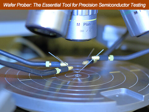
Wafer Prober: The Essential Tool for Precision Semiconductor Testing
Wafer probers play a crucial role in semiconductor manufacturing. They enable manufacturers to test the functionality of chips on a wafer before moving forward in the production process. By accurately assessing electrical properties, wafer probers help ensure the reliability of integrated circuits (ICs), which are vital for various technologies, from smartphones to medical devices. In this blog, we’ll explore what wafer probers are, how they work, and their importance in the semiconductor industry.
What Is a Wafer Prober?
A wafer prober is a machine used to test semiconductor wafers—thin slices of silicon or other semiconductor materials—during the chip manufacturing process. Wafers consist of many individual chips, also called dies, which are eventually packaged into ICs. Before this final packaging, each die must be tested for functionality, which is where wafer probers come into play.
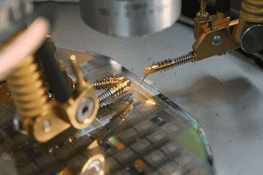
Wafer probers perform electrical tests by making contact with the circuits on the wafer through a specialized tool called a probe card. The probe card contains tiny needles that make contact with the pads on each die, allowing electrical signals to be transmitted. These signals determine if the circuits function as intended. This can identify any defects early in the manufacturing process.
Importance in Ensuring Chip Functionality
Wafer probers are essential because they help manufacturers detect faulty dies before proceeding with packaging. This ensures that only fully functional chips move forward. This can prevent costly errors in later production stages. Without wafer probing, defective chips could end up in devices. This may lead to malfunctions and poor performance in consumer electronics, medical instruments, and other applications.
Key Components of a Wafer Prober
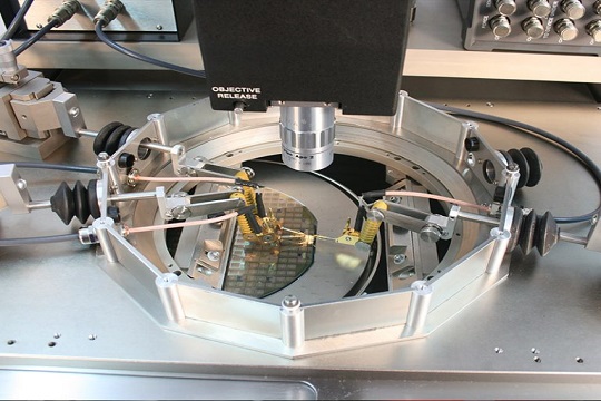
A wafer prober is composed of several critical components, each playing a specific role in the testing process:
- Probe Card: This component contains tiny needles that come into contact with the wafer’s test pads, allowing electrical signals to be transmitted.
- Wafer Chuck: The wafer chuck holds the wafer in place during testing. It typically uses a vacuum to secure the wafer to prevent any movement during the probing process.
- Microscope: Used for precise alignment of the probe card and the wafer. This ensures that the tiny needles accurately make contact with the correct points on the wafer.
- Positioning System: This system ensures the wafer is aligned correctly and moves the wafer under the probe card for testing each die.
Each of these components works together to ensure the wafer is tested accurately and efficiently. They together provide precise feedback about the wafer’s electrical performance.
How Wafer Probers Work
Wafer probing is a step-by-step process that requires mechanical precision and electrical testing. Here’s how it works:
- Loading the Wafer: The wafer is loaded onto the wafer chuck, which uses a vacuum to hold it securely in place.
- Positioning: The wafer is aligned under the probe card using a high-precision positioning system. This ensures that the probes make accurate contact with the wafer’s test pads.
- Probing: The probe card lowers onto the wafer, with its needles making contact with the wafer’s pads. Electrical signals are then sent through the probes, testing the wafer’s circuitry.
- Testing: The prober collects data on how the wafer’s circuits respond to the signals. If the wafer performs as expected, it is marked as functional. Otherwise, it is flagged as defective.
- Moving: The wafer is moved so that each die can be tested in sequence, ensuring that every chip on the wafer is evaluated.
Types of Wafer Probers
There are several types of wafer probers, each suited to different environments and applications:
- Manual Wafer Probers: Typically used in research and development settings, these probers are operated by hand. They are slower than automated systems but offer flexibility for testing new chip designs.
- Semi-Automatic Wafer Probers: These probers combine some level of automation with manual control. It makes them suitable for small-scale production environments.
- Fully Automatic Wafer Probers: Used in large-scale production. These machines can test wafers quickly and efficiently without human intervention. They are essential for high-volume manufacturing.
Each type of wafer prober has its own benefits. fully automatic probers offer the highest throughput and accuracy for large-scale semiconductor production.
Key Features of Wafer Probers
Wafer probers are equipped with several key features. These features make them indispensable in semiconductor manufacturing:
- Temperature Control: Wafer probers often come with temperature control feature. This allows them to test wafers under varying conditions. This is particularly important when assessing how a wafer performs under different environmental stress factors.
- High Precision: Wafer probers need to be highly precise to make contact with the tiny circuits on the wafer. The reason is that integrated circuit (IC) components shrinking in size. This requires advanced positioning systems and finely-tuned mechanical components.
- Automated Operation: In modern semiconductor fabs, automatic wafer probers are used to handle large volumes of wafers. They can run continuously. This reduces the need for manual intervention and improving production efficiency.
Applications of Wafer Probers in the Semiconductor Industry
Wafer probers are essential in several stages of semiconductor development and production:
- Research and Development (R&D): In R&D settings, wafer probers are used to test experimental chip designs. They help engineers identify and correct defects before mass production.
- Wafer Sorting: In mass production, wafer probers are used during the sorting process to identify defective dies. This ensures only functional chips are packaged into ICs.
- High-Volume Manufacturing: Automatic wafer probers are used to test thousands of wafers in large-scale production environments. This helps manufacturers maintain high-quality standards.
Advantages of Using Wafer Probers
Wafer probers offer several key advantages in semiconductor manufacturing:
- Improved Precision: Wafer probers provide highly accurate testing of tiny circuits. This helps manufacturers identify and correct issues early in the process.
- Increased Efficiency: Automated wafer probers can test large volumes of wafers quickly. This reduces downtime and improving production speed.
- Enhanced Yield: By identifying defective dies early, wafer probers help manufacturers improve their overall yield. This reduces waste and lowering production costs.
Importance of Wafer Probing in Semiconductor Manufacturing
Wafer probing is essential because it ensures that any defective wafers are identified early, reducing waste and cost. Without this testing, defective chips could be assembled into final products. This may result in product malfunctions or failures.
Wafer probers help manufacturers maintain high quality and yield. This is crucial in the competitive world of semiconductors. By identifying defective wafers before they go through costly packaging and assembly steps, manufacturers save time and resources while improving their final product's reliability.
Challenges and Future Trends in Wafer Probing
Wafer probing technology is continually evolving, but it still faces several challenges:
- Micro-Scale Probing: Chip components are shrinking. This makes precise contact with circuits becomes increasingly difficult.
- Contamination: Dust and debris can interfere with wafer testing. This makes cleanroom environments critical for accurate probing.
Looking ahead, wafer probers are likely to become even more automated and capable of handling smaller, more complex chips. New technologies, such as optical probing and improved positioning systems, will further enhance the accuracy and efficiency of wafer probers.
Conclusion
Wafer probers are an indispensable part of semiconductor manufacturing. They ensure the quality and functionality of the chips that power today’s technology. By testing wafers early in the production process, manufacturers can prevent defects, improve efficiency, and reduce costs. As technology continues to evolve, wafer probing will remain a key tool in the development of faster, more powerful, and more reliable electronic devices.
As a leading wafer manufacturer, we provide a wide range of wafers tailored for various applications, ensuring optimal performance for your semiconductor needs. If you're in the market for premium wafers, contact us today! Our team is ready to assist you in finding the perfect solution for your projects.