 +86-731-89578196
 [email protected]
- Home
- Our Company
-
Products
Sputtering Targets
- Industries
- Blog
- FAQ
- Contact Us
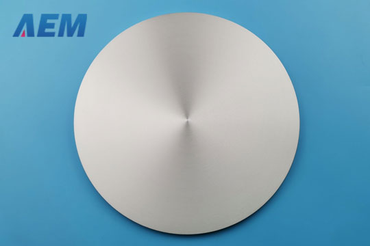
Sputtering Targets of AEM Deposition for LSI
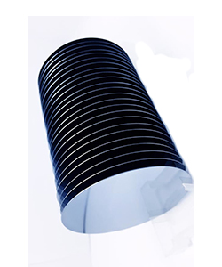
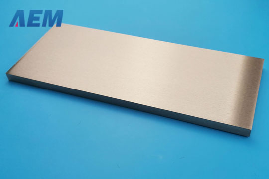
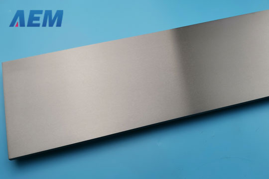
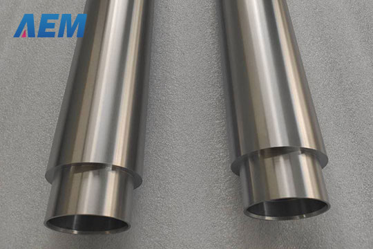
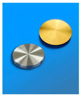
LSI's sputtering targets are used as indispensable materials for circuitry elements and wiring of VLSI and USLI semiconductors. The rapid advancement of integrity and the accompanying demands for faster devices require a broad range of high-quality sputtering targets.
The quality sputtering targets of the AEM Deposition have been enjoying a high reputation and reliance from our customers. The AEM Deposition Works is also praised because it is structured to develop the necessary technology and manufacture the sputtering targets promptly to meet the semiconductor industry's continually changing technology needs.
The sputtering targets manufactured at the AEM Deposition are used in various parts of VLSI and ULSI semiconductors such as gate elements (Ti, W-Si, etc.), barriers(Ti, Ta, W-Ti, etc.), metallization(Cu, Al-Alloy, etc.), and contacts(Ti, Al, etc.). Among others, Cu, Cu-Alloy, Ta, and other particular sputtering targets that are presently spotlighted as the newest materials for semiconductors are highly acclaimed. With speed and quality as its priority, the AEM Deposition also develops a wide range of technology spurred by the demand for more layers in the semiconductor circuitry while maintaining a close relationship with the customer as well as the sputtering equipment manufacturers. The development of next-generation materials for semiconductors such as ferroelectric materials is also energetically conducted at the AEM Deposition.


