Copper Sputtering Targets (Cu)
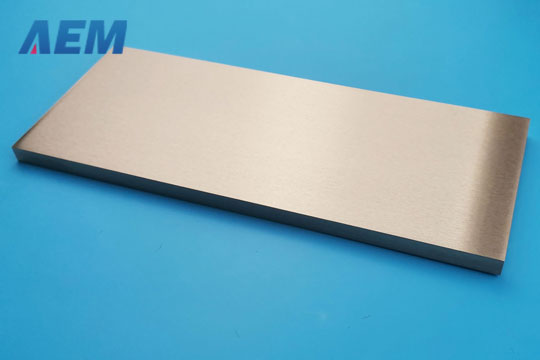

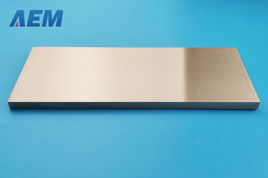
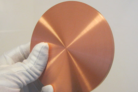
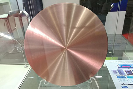
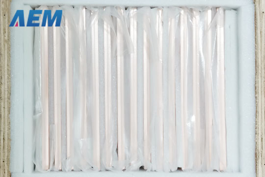
| Material Type | Copper |
| Symbol | Cu |
| Atomic Weight | 63.546 |
| Atomic Number | 29 |
| Color/Appearance | Copper, Metallic |
| Thermal Conductivity | 400 W/m.K |
| Melting Point (°C) | 1,083 |
| Coefficient of Thermal Expansion | 16.5 x 10⁻⁶/K |
| Theoretical Density (g/cc) | 8.92 |
| Z Ratio | 0.437 |
| Sputter | DC |
|
Max Power Density* (Watts/Square Inch) |
200 |
| Type of Bond | Indium, Elastomer |
| Comments | Adhesion poor. Use interlayer (Cr). Evaporates using any source material. |
Copper Sputtering Targets
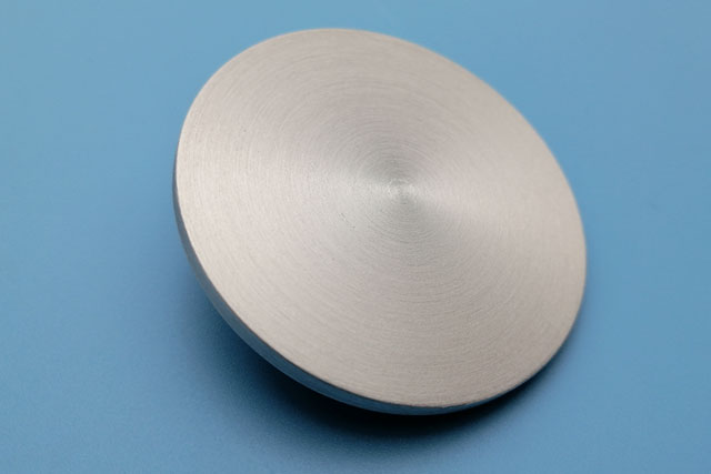
Copper is a ductile metal with very high thermal conductivity, electrical conductivity, ductility, corrosion resistance. A freshly exposed surface of pure copper has a reddish-orange color. High-purity copper is used as various wires in the electrical and electronics industry, bonding wires for electronic packaging, high-quality audio cables and integrated circuits, liquid crystal display sputtering targets, and ion plating. It is also an indispensable valuable material in atomic energy, rockets, missiles, aviation, space navigation, and metallurgical industries. AEM offers high purity OFC, Cupronickel, and alloy products as per requirement.
Copper Sputtering Targets Information
Copper Sputtering Targets
Purity: 99.99-99.9999%;
Circular: Diameter <= 14 inch, Thickness >= 1mm;
Block: Length <= 32 inch, Width <= 12 inch, Thickness >= 1mm;
Targets Type: Planar sputtering target, Rotary sputtering target.
Copper Sputtering Targets Analysis
AEM Deposition manufacture copper sputtering targets with high purity. The highest purity can reach to 99.9999%. The significant benefits are that your films possess an outstanding level of electrical conductivity and minimized particle formation during the PVD process. The analytical methods we use includes:
1. Metallic elements were analyzed using ICP-OES.
2. Gas elements were analyzed using LECO.
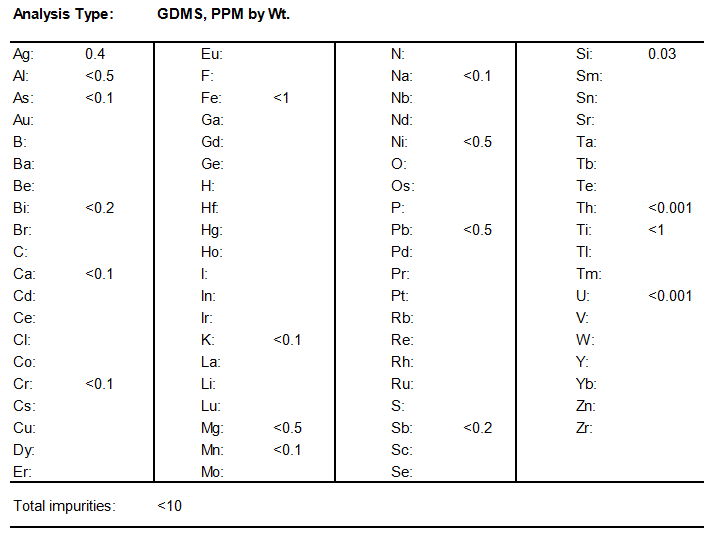
Below form is a Certificate of Analysis (COA) for 99.999% high purity Copper Sputtering Target:
More Information on Copper Sputtering Targets
Applications• Electronics• Semiconductor • Flat panel displays |
Features• Competitive pricing• High purity and density • Grain refined, Engineered microstructure ( the average grain size < 50 um) • Semiconductor grade |
Manufacturing Process• Melting and castingElectrical resistance furnace - Semi-continuous casting (VIM&EB) • Grain refinement Thermomechanical treatment (Forging, Rolling, Annealing) • Cleaning and final packaging - Cleaned for use in vacuum Protection from environmental contaminants Protection during shipment |
Options
• 99.99% minimum purity
• Smaller sizes also available for R&D applications
• Sputtering target bonding service
|
Related Products of Copper Sputtering Targets
|
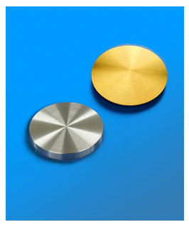
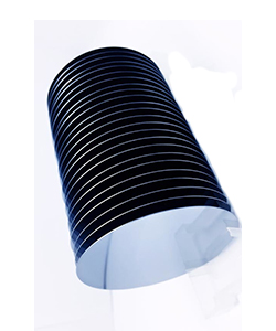
Ceramic Sputtering Targets Copper Aluminum Oxide Sputtering Target |
||
|
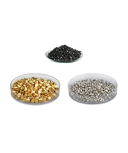
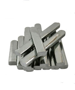
Evaporation Materials Copper Evaporation Pellet |
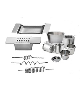
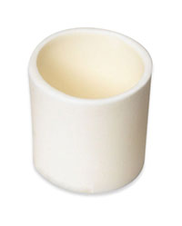
Crucibles Copper Crucible |
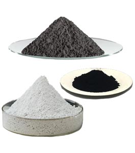
Metal Powders Copper Powder |
 Click to download datasheet about Copper Sputtering Targets (Cu)
 Unable to find the required data sheet? Click here to send an email and get it.
 Click here to get answers to Frequently Asked Questions (FAQ).
Related Products
FREE QUOTE


