Sputtering Targets
Evaporation Materials
Evaporation Sources
High Purity Materials
Thin Film Substrates
Crytstal Materials
 +86-731-89578196
 [email protected]
Sputtering Targets
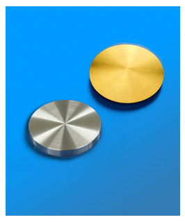
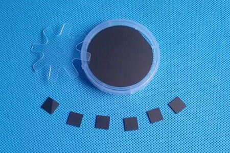

AEM is a leading manufacturer of high-quality germanium wafers. With years of experience and state-of-the-art facilities, we deliver pure, precise, and reliable germanium wafers. Our commitment to excellence ensures our products meet the highest industry standards for various applications.
From infrared optics to semiconductor devices, AEM's germanium wafers are trusted for their superior performance and reliability. Our dedication to innovation drives us to continuously improve our processes and expand our product offerings to meet the evolving needs of our customers.
| Size | 10x3, 10x5, 10x10, 15x15, 20x 15, 20x 20,Dia 1'', Dia 2'', Dia 4", Dia 6" |
|---|---|
| Thickness | 0.33mm, 0.43mm 0.5mm, 1.0mm |
| Polished | SSP or DSP |
| Orientation | <100>,<110>, <111> |
| Redirection Precision | ±0.5° |
| Ra: | ≤5Å(5µm×5µm) |
| Material | Germanium | ||
|---|---|---|---|
| Growth Method | CZ | ||
| Structure | M3 | ||
| Lattice (A) | a=5.65754 | ||
| Melting Point | 937.4℃ | ||
| Density(g/cm3) | 5.323 g/cm3 | ||
| Doped Material | undoped | Sb-doped | In/Ga-doped |
| Type | / | N | P |
| Resistivity | >35 Ωcm | 0.05 Ωcm | 0.05~0.1 Ωcm |
| Thermal-expans | <4 x10³/cm2 | <4 x10³/cm2 | <4 x10³/cm2 |
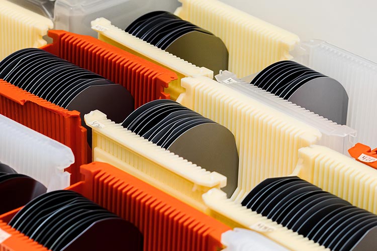
Our germanium wafers are renowned for their exceptional purity, ensuring optimal performance in even the most demanding applications.
AEM's advanced manufacturing processes guarantee precise dimensions and tolerances, delivering wafers that meet the strictest specifications.
We adhere to rigorous quality control standards, ensuring that every germanium wafer we produce meets the highest industry benchmarks.
AEM offers a wide range of germanium wafer options to meet your specific needs, whether you require wafers for infrared optics, semiconductor devices, or other applications.
With our global distribution network, AEM can supply germanium wafers to customers worldwide, ensuring timely delivery and reliable service.
A narrow molten zone is passed through a germanium ingot, causing impurities to concentrate at the zone's boundaries. This process is repeated multiple times, resulting in a highly purified germanium ingot.
A seed crystal is dipped into a molten germanium pool. As the seed is slowly withdrawn, the molten germanium solidifies onto the seed, forming a single-crystal ingot with a controlled orientation.
The ingot is sliced into wafers using a diamond saw. The cutting process is carefully controlled to minimize damage to the wafer surfaces.
The wafer surfaces are ground using abrasive materials to remove material and create a flat, smooth surface. Grinding is typically performed in multiple stages, starting with coarser abrasives and gradually progressing to finer ones.
Chemical etching is used to selectively remove material from the damaged or contaminated areas of the wafer. The etching process is carefully controlled to avoid excessive material removal and ensure a smooth, defect-free surface.
The wafers are subjected to a series of cleaning steps, including chemical baths and rinsing. Then, wafers are inspected for defects such as scratches, pits, and particles. If required, the wafers are polished to achieve a mirror-like finish on one or both sides.
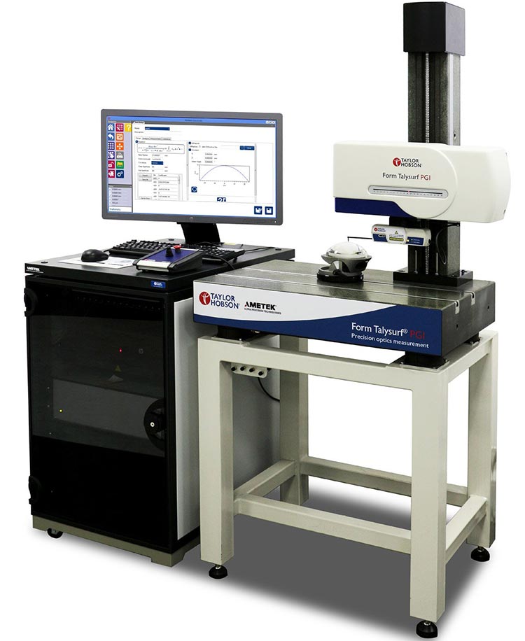
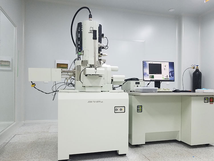

Germanium is highly transparent to infrared radiation, making it ideal for infrared optics, detectors, and sensors.

Germanium has a low absorption coefficient for infrared wavelengths, allowing for efficient transmission and detection of infrared signals.

Germanium has a high carrier mobility, which means that electrons and holes can move through the material with relative ease. This makes it suitable for high-speed electronic devices.
Germanium has a relatively low bandgap, which allows for efficient carrier generation and recombination. This property is essential for semiconductor devices such as transistors and diodes.

Germanium is a relatively strong and hard material, making it resistant to mechanical stress and abrasion. This is important for applications where the wafers are subjected to physical handling or environmental factors.

Germanium has a low thermal expansion coefficient, which means it experiences minimal dimensional changes with temperature fluctuations. This property is crucial for applications where precise dimensional stability is required.

Germanium has been shown to be biocompatible, making it suitable for certain biomedical applications.


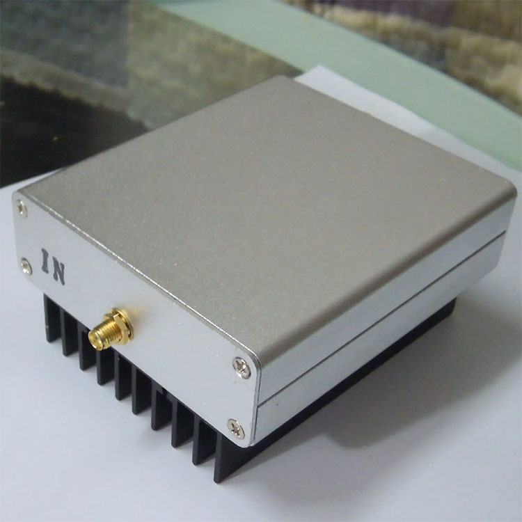


Germanium wafers serve as the substrate for high-efficiency multi-junction solar cells, especially in space applications. Germanium's compatibility with III-V semiconductor materials (like GaAs and InP) allows for the fabrication of multi-junction solar cells, which are used in satellites and space missions for power generation due to their high efficiency in converting sunlight into electricity.

Germanium wafers are used in the production of optoelectronic sensors that detect light signals and convert them into electrical signals. These sensors are widely used in optoelectronic control systems and photometric measurement instruments. The high sensitivity of germanium to infrared and near-infrared light makes it ideal for these applications, providing precise light detection in a variety of industrial and scientific fields.
Packaged with class 100 clean bag or wafer container in a class 1000 clean room.
A germanium wafer is a thin, circular slice of germanium crystal used as a substrate in semiconductor and optoelectronic applications.
Yes, germanium is often combined with silicon in Silicon-Germanium (SiGe) technology for improved performance.
Common dopants for germanium include arsenic, antimony (n-type), and boron (p-type).
Yes, germanium wafers can be recycled, and the germanium material can be reclaimed and reused in new wafers.
Yes, germanium is prone to oxidation, which can form a thin native oxide layer on the wafer surface.
Germanium is generally considered non-toxic in its wafer form, but some germanium compounds can be toxic if ingested or inhaled in large amounts.
Germanium is alloyed with silicon in SiGe technology to improve transistor performance in high-speed and RF applications.
Germanium's high sensitivity to temperature changes makes it useful in temperature-sensitive devices like thermistors.
Common defects in germanium wafers include dislocations, twins, precipitates, and surface scratches. These defects can impact the performance of the wafer in various applications.
Please be advised that customised specification germanium wafers require approximately 3-4 weeks for shipping. If the order is for a regular specification and we have stock, it can be shipped in 1-2 weeks. Please also understand that if transportation volume accumulates during holidays, the delivery time may be slower.
| Superconducting Substrates | |
| Magnetic Ferroelectricity Substrates | |
| Semiconductor Wafers | |
| GaN Thin Film Substrates | |
| Halide Substrates | |
| Ceramic Substrates | |
| Metal Substrates |