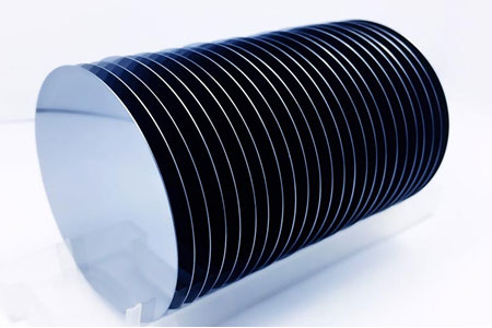
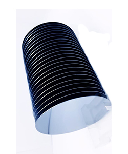
Gallium Antimonide Wafer
Gallium antimonide (GaSb) is a vital semiconductor material of III-V element family. It's also the critical material to uncooled medium-long-wave infrared detectors and focal plane arrays. The infrared detectors have long life, high sensitivity, and reliability. It's widely used in infrared laser, infrared detector, infrared sensor, thermal photovoltaic cell.
Gallium Antimonide Wafer Physical Properties
|
Material |
GaSb |
|
Growth Method |
LEC, VGF, VBG |
|
Lattice (A) |
a=6.094 |
|
Structure |
M3 |
|
Melting Point |
712℃ |
|
Density(g/cm3) |
5.53 g/cm3 |
|
Doped Material |
undoped |
Te-doped |
Zn-doped |
|
Type |
P |
P |
N |
|
Carrier Concentration (cm-3) |
(1-2) x 1017 |
(5-100) x 1017 |
(1-20) x 1018 |
|
Mobility (cm2v-1s-1) |
600-700 |
200-500 |
2000-350 |
|
EPD (Average) |
<2000/cm2 |
<2000/cm2 |
≤2000 /≤500/cm2 |
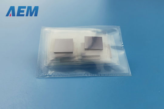
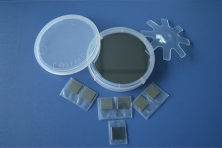
Gallium Antimonide Wafer Specification
|
Size |
10mm x 10 mm, 10 mm x 5 mm,2'' Dia, 3'' Dia (customized sizes are available) |
|
Thickness |
500um, 600um, 800um (Tolerance: ±25um) |
|
Polished |
SSP or DSP |
|
Orientation |
<100>, <111> |
|
Redirection Precision |
±0.5° |
|
Primary Flat Length |
16±2 mm, 22±2 mm, 32.5±2 mm |
|
Scondary Flat Length |
8±1 mm, 11±1 mm, 18±1 mm |
|
TTV |
<10 um, <20 um |
|
Bow |
<10 um, <20 um |
|
Warp |
<15 um, <20 um |
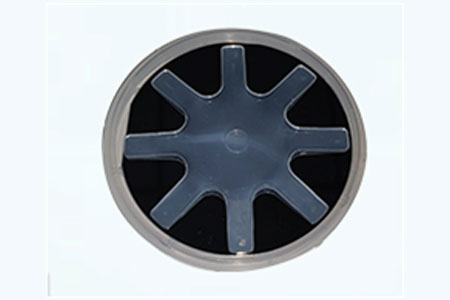
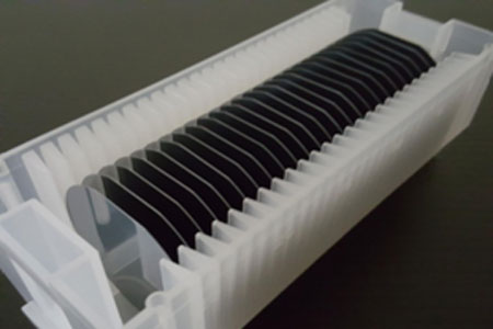
Gallium Antimonide Wafer Package
Packaged with class 100 clean bag or wafer container in a class 1000 clean room.
Related Products of Gallium Antimonide Wafer


 Click to download datasheet about Gallium Antimonide Wafer (GaSb)
 Unable to find the required data sheet? Click here to send an email and get it.
 Click here to get answers to Frequently Asked Questions (FAQ).