


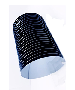
Question: How to choose the thickness of substrates & wafers?
Answer: The thickness of the wafers is always determined by the automated strength of the materials used, which means the wafer should be thick enough so that it does not crack during handling. So as to reduce cost per die, producers want to exploit the number of dies made out of a single wafer. As a result of the limitation of wafer dicing, dies only contain a square or rectangular shape. That makes it a computationally intricate difficult without an analytical answer, which is dependent on both of their aspect ratios, square or even rectangular, and the capacity of the dies, along with other respects such as the space covered by alignment and text structures, and the scribe line size. Orientation is always very of great value since many of a single crystal’s mechanical and electronic things are anisotropic, making them directionally dependent. Ion establishment depths be subject to on the crystal orientation of the wafer because each direction provide unique paths for transport.
Question: What is the silicon wafer used for?
Answer:
1. Semiconductor
Even though other conductors are employed in more particular applications, silicon is the best and the most used semiconductor due to its extreme mobility both at high temperatures and at room temperature. What makes Silicon an outstanding option in electronic devices is because its electrical currents can pass via the silicon conductors much quicker compared to other conductors.
2. Silicon Wafers In Electronic Devices
Semiconductors such as the silicon wafer can be used in the production of both chips and microchips in electronic gadgets. Due to the uniqueness of the electrical currents via silicon wafers, these semiconductors are used in creating ICs (integrated circuits). The ICs act as commands for specific actions in various electronic devices. The Silicon wafer is the main element in integrated circuits. Simply put, integrated circuits are a composite of a variety of electronic elements that are brought together to perform a particular function. Silicon is the key platform for semiconductor gadgets. A wafer is just but a thin slice of the semiconductor material that acts as a substratum for microelectronic devices fitted in and above the wafer. Silicon wafers are used in computers, smartphones, and mobile devices and even in the tire pressure sensor system. Manufacturing of the silicon wafer is an incredibly vital part of the establishment and expansion of a broad range of technological advancements.
Not finding what you need?
Just send your question to [email protected].
And we'll reply you as soon as possible.