 +86-731-89578196
 [email protected]
- Home
- Our Company
-
Products
Sputtering Targets
- Industries
- Blog
- FAQ
- Contact Us
Application and Introduction of Sputtering Target for Semiconductor Chip
views, Updated: 2021-09-17
Semiconductor chips have high technical requirements and high prices for sputtered targets. Their requirements for sputtered targets' purity and technology are higher than flat-panel displays, solar cells, and other applications. Semiconductor chips set extremely strict standards for the purity of sputtering target metal materials, internal microstructure, and other aspects. If the impurity content of the sputtering target is too high, the film formed can't meet the required electrical performance. In the sputtering process, it is easy to form particles on the wafer, resulting in a short circuit or damage of the circuit, which seriously affect the performance of the film. Generally speaking, chip manufacturing requires the highest purity of sputtering target metal, which is usually 99.9995% (5N5) or more, while flat-panel display and solar cell require 99.999% (5N) or 99.995% (4N5) or more, respectively.
Semiconductor sputtering target application
The sputtering target is used for the fabrication of the barrier layer and the packaging metal wiring layer. In the wafer manufacturing process, the target material is mainly used to make the wafer conductive layer, barrier layer, and metal grid. In the chip packaging process, the sputtering target material is used to generate the metal layer under the bump, wiring layer, and other metal materials. Although the amount of target materials used in wafer manufacturing and chip packaging is small, according to SEMI statistics, the cost of target materials in wafer manufacturing and packaging process accounts for about 3%. However, the quality of sputtering target materials directly affects the uniformity and performance of conductive layer and barrier layer, and further affects chip transmission speed and stability, so sputtering target materials are the core raw materials for semiconductor production one of the materials.
Sputtering target for semiconductor
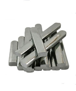
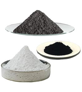
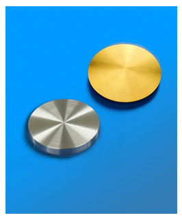
In the process of wafer fabrication, sputtering targets for semiconductors are mainly used for the fabrication of the conductive layer, the barrier layer, and metal grid, which are mainly used for aluminum, titanium, copper, tantalum, and other metals. AEM Deposition, as a professional sputtering target manufacturer, provides pure metal sputtering targets suitable for semiconductors. See the table below:
| Aluminum Sputtering Target | Copper Sputtering Target | Tantalum Sputtering Target |
The metal target materials for chip packaging are similar to wafer fabrication, including copper, aluminum, and titanium. Among them, the main metal targets used in the fabrication of the conducting layer are aluminum sputtering target and copper sputtering target. The main metal targets used in the barrier layer are tantalum sputtering target and titanium sputtering target. The barrier layer has two main functions: one is to block and insulate to prevent the conductive layer metal from diffusing into the main material silicon of the wafer. The other is used as an adhesion for bonding metal silicon materials. Aluminum and titanium are used as thin-film materials for conductor and barrier layer for wafers above 110 nm technology node, copper and tantalum are used as thin-film materials for conductor and barrier layer for wafers below 110 nm technology node. With the reduction of the wafer manufacturing process, the proportion of copper target, tantalum target, and titanium target for metal grid continue to increase in the future.
In addition to semiconductor sputtering targets, AEM Deposition provides all kinds of pure metal sputtering targets, alloy sputtering targets, and ceramic sputtering targets. See the table below for further details. Interested friends can click the link below to go to the corresponding product page.
LATEST NEWS


