Substrates & Wafers for LED
views, Updated: 2021-09-27
The semiconductor layers in LED chips convert electrical current into light. They consist of an area of excess electrons (n-doped) and an area where there is a shortage of electrons (p-doped). When current is applied to the semiconductor layers, the electron distribution balances out. They radiate light in the form of photons. The remaining energy is emitted as heat, which must be reliably dissipated. Durable LED lights need reliable and robust components. With our molybdenum and MoCu substrates & wafers, the service life of 100,000 operating hours of the LED chip is easily achievable.
In the future, LEDs shine even brighter. And the operating temperatures rise. With molybdenum wafer substrates, for example, for use in sapphire- or silicon-based (Si) LED chips and the MoCu composites that we have developed especially for use in sapphire-based LED chips. AEM Deposition provides the optimum material for heat dissipation in its range.
Wafer substrates are bonded to the semiconductor layers of LED chips at temperatures of up to 800°C. The MoCu material specially developed by us for sapphire-based LEDs is tailored for the soldering process and long-term heat dissipation in LED chips. It has the same coefficient of thermal expansion as Al2O3. Al2O3 is the base material for both the sapphire wafer and the LED chip's ceramic carrier plate. The uniform thermal expansion of MoCu wafer, a sapphire substrate, and the ceramic base plate prevents defects in the semiconductor and solder layers.
The thermal conductivity (TC) of our MoCu material R670 for LED chips is 170 W/mK (at 20 °C ) and therefore higher than that of pure molybdenum (142 W/mK). The benefit to you: Even better heat dissipation in your sapphire-based LED chips.
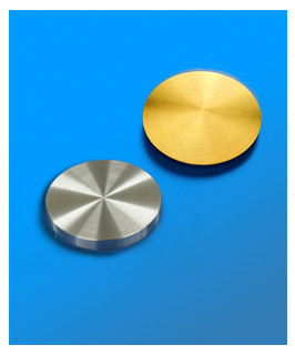
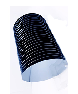
Our molybdenum and MoCu wafer substrates are available in thicknesses from 0.05 mm and diameters up to 300 mm (12 inches). Even diameters of 8 inches or more are not a problem for us. If you want to test, we would also be pleased to supply you with small sampling quantities. The roughness and evenness of wafer substrates have a decisive influence on the connection to the semiconductor. Contact us. We provide you customized surfaces for your process.
LATEST NEWS
2024-05-24
2023-10-17
2023-10-17
2023-09-15
2023-09-15
 +86-731-89578196
 [email protected]
