


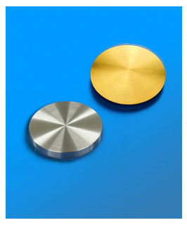
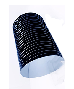
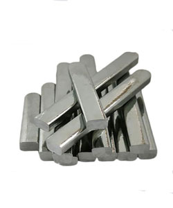
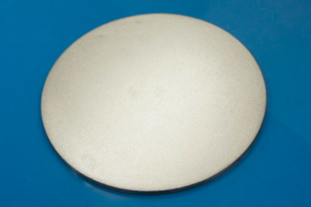
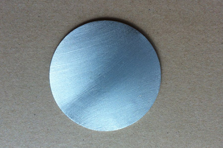
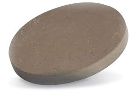
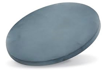
Terbium Sputtering Targets (Tb)
| Material Type | Terbium |
| Symbol | Tb |
| Atomic Weight | 158.92535 |
| Atomic Number | 65 |
| Color/Appearance | Silvery White, Metallic |
| Thermal Conductivity | 11 W/m.K |
| Melting Point (°C) | 1,356 |
| Coefficient of Thermal Expansion | 10.3 x 10⁻⁶/K |
| Theoretical Density (g/cc) | 8.27 |
| Z Ratio | 0.66 |
| Sputter | RF |
| UN Number | 2813 |
Terbium Sputtering Targets
Terbium is a silvery-white rare earth metal. It is malleable, ductile, and soft enough to be cut with a knife. It is relatively stable in the air than the earlier, more reactive lanthanides in the first half of the lanthanide series. Terbium exists in two crystal allotropes with a transformation temperature of 1289 ℃ between them. The 65 electrons of a terbium atom are arranged in the electron configuration [Xe]4f96s2. Usually, only three electrons can be removed before the nuclear charge becomes too great to allow further ionization, but in the case of terbium, the stability of the half-filled [Xe]4f7 configuration allows further ionization of a fourth electron in the presence of powerful oxidizing agents such as Fluorine gas.
Terbium Sputtering Targets Information
Terbium Sputtering Targets
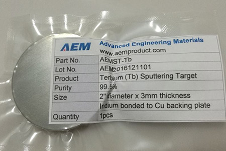
Purity: 99.9%;
Circular: Diameter <= 14 inch, Thickness >= 1mm;
Block: Length <= 32 inch, Width <= 12 inch, Thickness >= 1mm.
Due to these materials' highly reactive nature, packaging in oil is required to reduce the opportunity for oxidation or other reaction.
More Information on Terbium Sputtering Targets
Applications• Electronics• Semiconductor • Flat panel displays |
Features• Competitive pricing• High purity • Grain refined, Engineered microstructure • Semiconductor grade |
Manufacturing Process• RefiningThree-layer electrolytic process • Melting and casting Electrical resistance furnace - Semi-continuous casting • Grain refinement Thermomechanical treatment • Cleaning and final packaging - Cleaned for use in vacuum Protection from environmental contaminants Protection during shipment |
Options• 99.9% minimum purity• Smaller sizes also available for R&D applications • Sputtering target bonding service |
Related Products of Terbium Sputtering Targets
|
Ceramic Sputtering Targets |
||
|
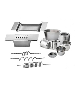
Evaporation Materials N/A |
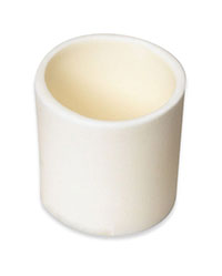
Crucibles N/A |
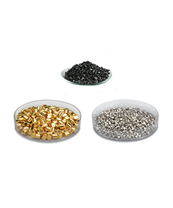
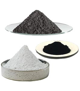
Metal Powders N/A |
 Click to download datasheet about Terbium Sputtering Targets (Tb)
 Unable to find the required data sheet? Click here to send an email and get it.
 Click here to get answers to Frequently Asked Questions (FAQ).
Related Products
FREE QUOTE