


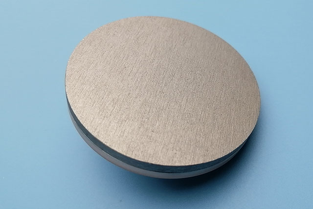
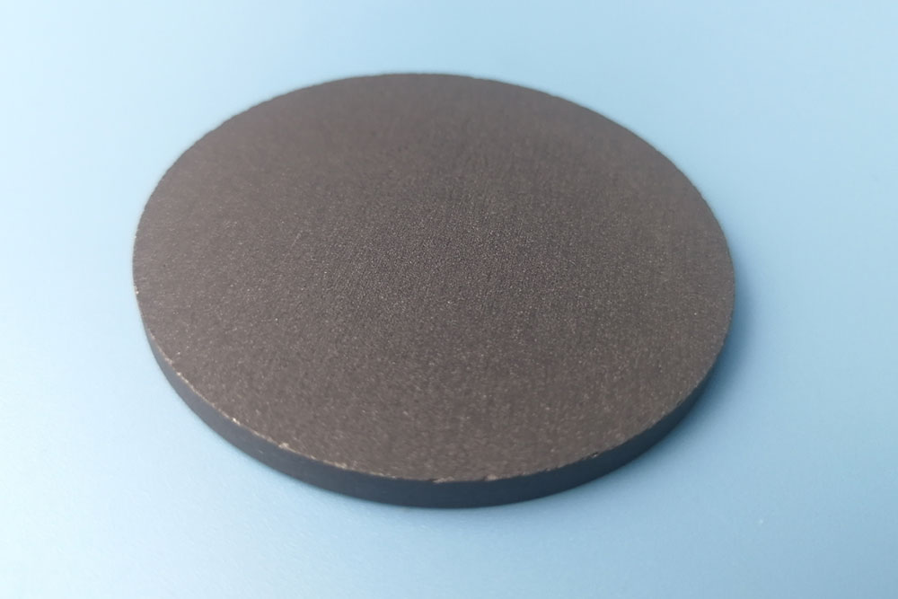
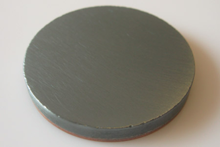
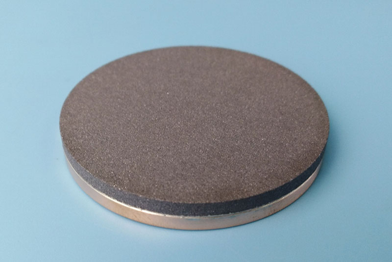
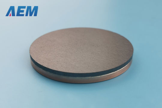
Bismuth Selenide Sputtering Targets (Bi2Se3)
| Material Type | Bismuth Selenide |
| Symbol | Bi2Se3 |
| Color/Appearance | Black, Crystalline Solid |
| Melting Point (°C) | 710 |
| Theoretical Density (g/cc) | 6.82 |
| Z Ratio | **1.00 |
| Sputter | RF |
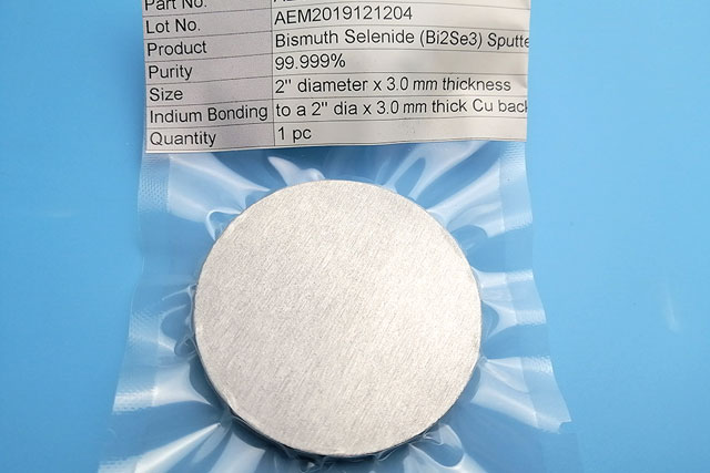
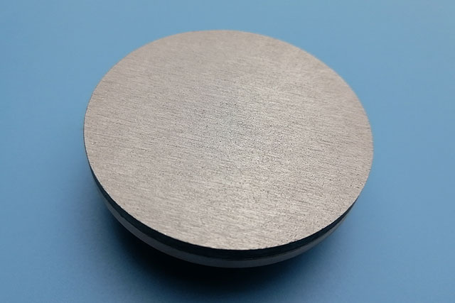
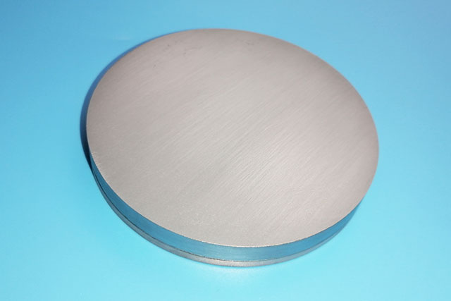
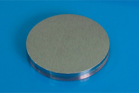
| Type of Bond | Indium, Elastomer |
| UN Number | 3283 |
| Comments | Co-evap from 2 sources or sputter. |
Bismuth Selenide Sputtering Targets
Bismuth selenide (Bi2Se3) is a gray powder, a bismuth and selenium compound, also known as bismuth(III) selenide. It is a semiconductor and a thermoelectric material. At the same time, perfect stoichiometric bismuth selenide should be a semiconductor (with a gap of 0.3 eV). Naturally occurring selenium vacancies act as electron donors, and it often acts as a semimetal.
Bismuth Selenide Sputtering Targets Information
Bismuth Selenide Sputtering Targets
Purity: 99.99%;
Circular: Diameter <= 14 inch, Thickness >= 1mm;
Block: Length <= 32 inch, Width <= 12 inch, Thickness >= 1mm. Hazardous shipping charges may apply.
Indium bonding is recommended for this material due to its characteristics not amenable to sputtering like brittleness and low thermal conductivity. This material has a low thermal conductivity and susceptible to thermal shock.
More Information on Bismuth Selenide Sputtering Targets
Applications• Chemical Vapor Deposition (CVD)• Physical Vapor Deposition (PVD) • Semiconductor • Optical |
Features• High purity• Custom sizes available |
Manufacturing Process• Manufacturing - Cold pressed - Sintered, Elastomer bonded to backing plate
• Cleaning and final packaging, Cleaned for use in vacuum, |
Options
• 99.99% minimum purity
• Smaller sizes also available for R&D applications
• Sputtering target bonding service
|
Related Products of Bismuth Selenide Sputtering Targets
|
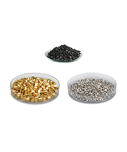
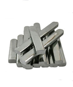
Pure Metal Sputtering Targets |
|
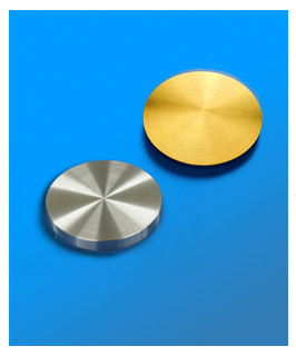
Ceramic Sputtering Targets |
|
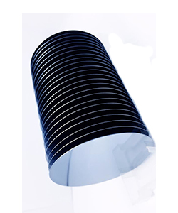
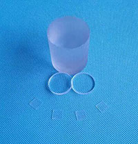
Evaporation Materials |
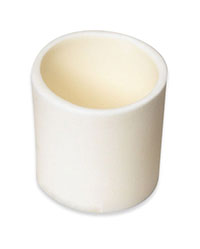
Crucibles N/A |
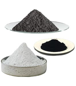
Metal Powders N/A |
 Click to download datasheet about Bismuth Selenide Sputtering Targets (Bi2Se3)
 Unable to find the required data sheet? Click here to send an email and get it.
 Click here to get answers to Frequently Asked Questions (FAQ).
Related Products
FREE QUOTE