Sputtering Targets
Evaporation Materials
Evaporation Sources
High Purity Materials
Thin Film Substrates
Crytstal Materials
 +86-731-89578196
 [email protected]
Sputtering Targets
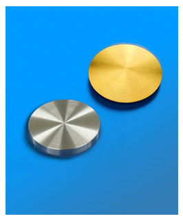
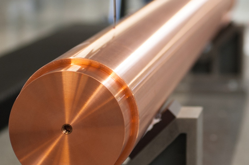
AEM is a renowned industry leader and trusted manufacturer specializing in cutting-edge sputtering targets. We not only manufacture and sell custom small targets for experimental research and production development in over 500 materials, but we also produce large tube targets or planar targets for flat panel displays or other fields to meet any of your specific requirements.
Sputtering targets are key raw materials used in the process of manufacturing thin films using physical vapor deposition technology (PVD). High-speed ion beams bombard the solid surface to cause atoms to leave the solid to form thin films. They are mainly usedin integrated circuits and semiconductors. Display, semiconductor chip, photovoltaic solar energy industry, storage, low-emissivity glass in construction/automotive glass industry, decorative plating and other fields.
You can check the details information of specific category as below:
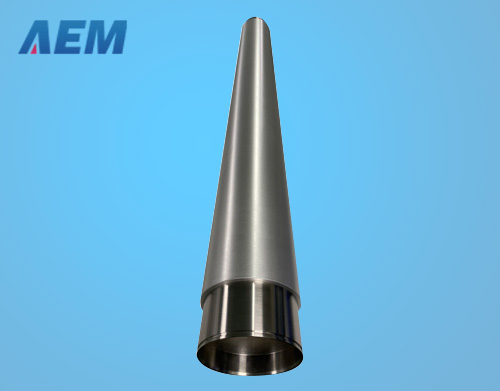
Titanium (Ti) Rotary sputtering targets supplier, AEM produces 99.5% to 99.999% purity of rotatable titanium targets with customiz...
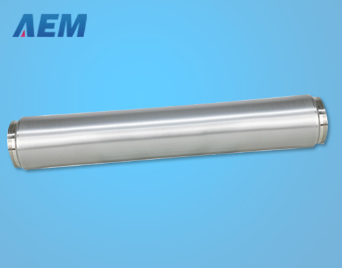
Chromium (Cr) Rotary sputtering targets supplier, AEM produces 99.5% to 99.95% purity of rotatable chromium targets with customize...
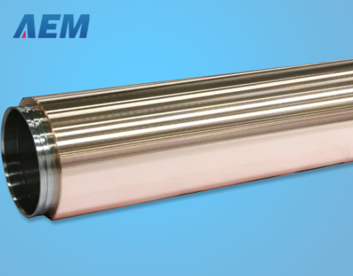
Copper (Cu) Rotary sputtering targets have excellent properties of high thermal conductivity, electrical conductivity, ductility, ...
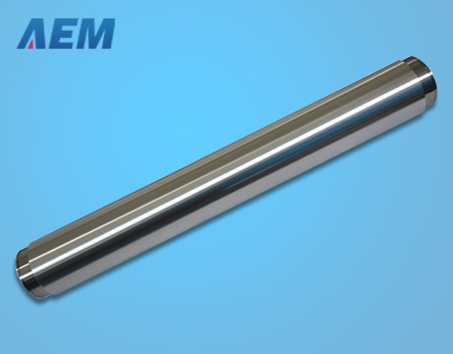
AEM produces Aluminum rotary sputtering targets with customized sizes and shapes. These are used for conductive films, capacitor f...
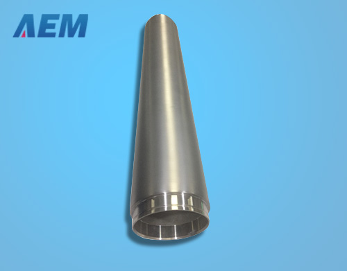
AEM produces 99.95% purity of Niobium rotary sputtering targets with customized sizes and shapes. Which are used for optical glass...
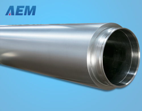
AEM produces 99.95% purity of Molybdenum rotary sputtering targets with customized sizes and shapes. Which are used for vacuum coa...
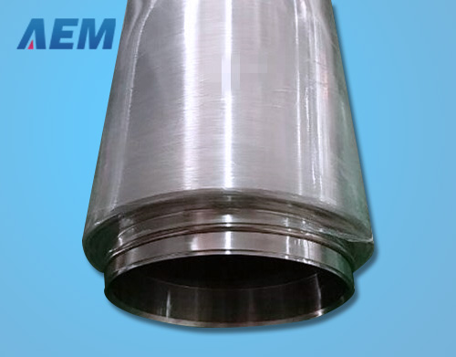
Zirconium (Zr) Rotary Sputtering Targets have excellent hardness, ductility, and corrosion resistance. AEM provides it with custom...
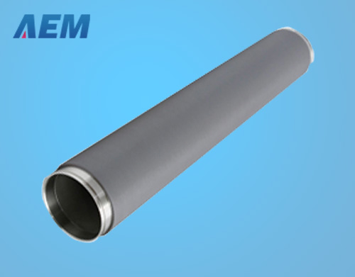
Silicon (Si) Rotary Sputtering Targets have two types of forms Monocrystalline and polycrystalline. We can produce it in customize...
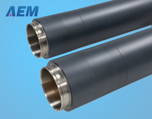
Indium Tin Oxide (ITO) Rotary Sputtering Targets are widely used to form electrically transparent thin films. AEM produces it with...
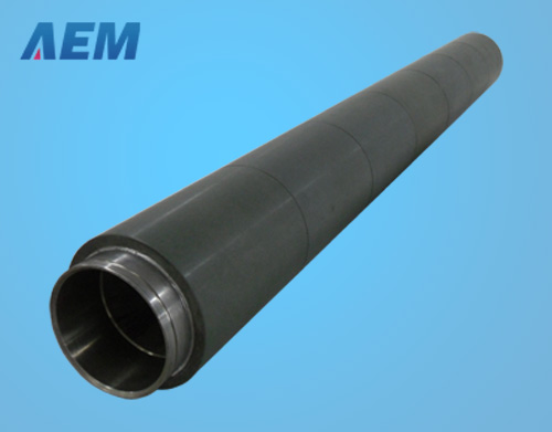
AZO Rotary Sputtering Targets are widely used in thin-film solar cells, Low-E coated glass, automotive-coated glass, and flat pane...
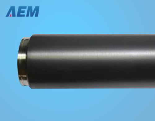
Titanium Oxide (TiOx) Rotary Sputtering Targets are widely used in photovoltaic glass, optical glass, construction, and automotive...
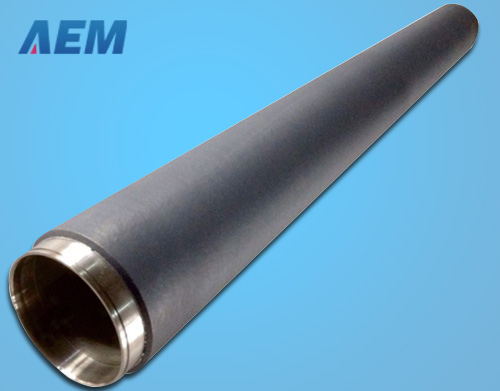
AEM produces Niobium oxide rotary sputtering targets with customized sizes and shapes. These are used for Low-E glass film systems...
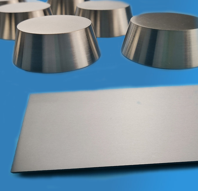
We offer a diverse range of sizes and shapes for our targets, including planar targets, rotating targets, tube targets, and more, providing you with the flexibility to choose according to your specific needs.
We can customize production based on your specific requirements for size, shape, and material.
We use core technologies such as plasma spraying, ceramic sintering, and vacuum smelting to produce targets, and provide sputtering targets and a complete set of equipment and technologies for plasma spraying and casting rotating targets.
We ensure the quality of raw materials for the target material, oversee the production process, maintain our own inspection system, and hold international certification in the form of ISO 9001.
If you have any questions about choosing the right sputtering targets, you can contact our sales team directly. Submit the form below and you will get a quote within one working day.
Material Selection: Choose a material of appropriate purity, typically a metal or compound, as the raw material for the sputtering target. The material selection is based on the specific requirements of the final application, such as conductivity, optical properties, etc.
Powder Preparation: Process the chosen raw material into powder form. This can be achieved through methods like mechanical alloying, chemical vapor deposition, ensuring uniformity and fine particle size of the powder.
Mixing and Compaction: Mix the powder with potential additives to adjust the properties of the sputtering target. The mixed powder is then compacted through methods like cold isostatic pressing or uniaxial pressing to form a green body.
Sintering: Subject the pressed green body to sintering, a process where the powder particles bond together to form a dense body. Sintering temperature and time are optimized based on the material's nature and requirements.
Machining: Perform machining operations on the sintered body, including cutting, grinding, and polishing, to achieve the final shape and surface quality according to specifications.
Quality Inspection: Conduct quality inspections, encompassing composition analysis, density measurements, structural analysis, etc., to ensure the sputtering target meets specified standards.
Coating (Optional): Apply coatings to the sputtering target based on specific application needs, enhancing corrosion resistance or improving optical properties, for instance.
Packaging and Delivery: Properly package the prepared sputtering target to prevent contamination and damage. Deliver the product to the customer or proceed to the next manufacturing step.
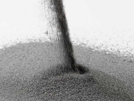


Material Preparation:: Select high-purity raw materials, usually metals or compounds, as the base for sputtering targets. Material selection is based on specific requirements for the final application, such as electrical conductivity, optical properties, etc.
Powder Preparation: Process the chosen raw materials into a powdered form. This can be achieved through methods like mechanical alloying, chemical vapor deposition, ensuring uniformity and fine particle size of the powder.
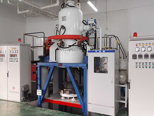
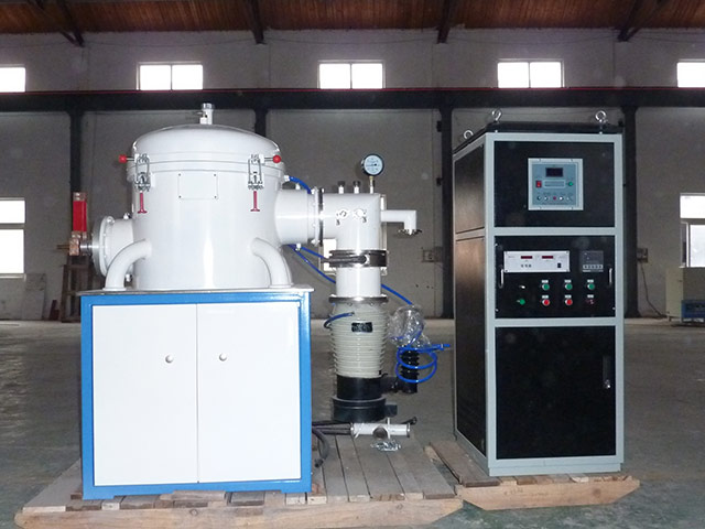
Vacuum Melting: Melt the powder in a high vacuum environment, typically using an arc furnace or induction heating furnace. During the melting process, the material is evaporated and condenses onto a cooled surface, forming a uniformly dense ingot.
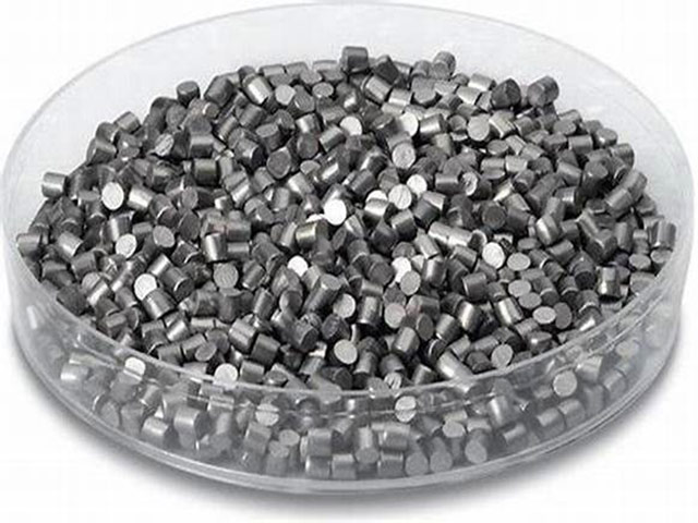
Ingot Formation: The powder gradually forms an ingot through cooling and solidification. This ingot possesses high purity and density, serving as the starting point for subsequent processing.
Heat Treatment: Subject the ingot to heat treatment to optimize crystal structure and enhance material mechanical properties. Heat treatment temperature and time are precisely controlled based on specific requirements.
Processing and Finishing: Mechanically process the heat-treated ingot, including cutting, grinding, and polishing, to achieve the final shape and surface quality of the sputtering target.
Quality Inspection: Conduct quality inspections, including composition analysis, density measurements, and microstructure analysis, to ensure the sputtering target complies with specified standards.
Coating (Optional): Depending on the specific application needs, apply coatings to the sputtering target to enhance corrosion resistance or improve optical properties, among other factors.
Packaging and Delivery: Properly package the prepared sputtering target to prevent contamination and damage. Deliver the product to the customer or proceed to the next manufacturing step.


When it comes to selecting a sputtering targets, a thorough evaluation of several critical factors is paramount to ensure it aligns perfectly with your requirements. Let’s delve into each of these essential considerations:
Intended application: Selecting the right target material first requires an in-depth understanding of the application requirements of the film. Different applications (e.g., photovoltaics, semiconductors, decorative coatings) have different requirements for the electrical, optical and mechanical properties of thin films. Therefore, defining the application purpose and performance requirements of the film is the first step in target selection.
Evaluate target properties: After determining the application needs of the film, the target needs to be selected based on its purity, compositional homogeneity, size and shape. For example, for highly transparent optical films, it is particularly important to select targets with uniform composition and high purity. For large-area coatings, target size and shape uniformity are critical to improving deposition efficiency and film uniformity.
Consider cost-effectiveness: When selecting targets, there is also a balance of cost-effectiveness to consider. While high-quality targets may cost more, they may be more economical in the long run by providing superior film performance and longer service life.
Equipment and target compatibility: Ensure that the specification, size and shape of the target purchased matches the equipment requirements, and that the physical and chemical properties of the selected material are suitable for the required application and equipment to ensure that it can be loaded and used correctly.
Sputtering method: For reactive sputtering or the preparation of thin films of specific compounds, targets matching the gases used in the sputtering process are required. High-frequency sputtering or magnetron sputtering are generally more suitable for using pure, homogeneous targets for stable deposition. Some sputtering methods may require targets of special shapes, sizes, or structures, such as magnetron sputtering, which improves target utilization. The choice of sputtering method needs to take into account the physical and chemical properties of the target to ensure that it is compatible with the process and that the desired film properties are obtained.
Conductivity: The higher the purity of the target, the higher the conductivity. In semiconductor and conductive film applications, trace impurities can significantly affect the conductivity of the material. High purity targets reduce these impurities and provide higher conductivity, which is critical for high performance electronics.
Specialized resources and guidance are critical to selecting the right target, and by partnering with AEM, a supplier of specialized sputtering targets, we will utilize our years of technical knowledge and experience to help you more accurately select the target that meets your needs.
As a major raw material used in coating, the inherent characteristics of the target—such as its shape, purity, density, porosity, grain size, and bonding quality—have a significant impact on both film quality and sputtering rate. Superior-quality targets not only ensure top-notch film quality but also contribute to extending the lifespan of Low-e products. More importantly, they can reduce production costs, enhance production efficiency, and yield substantial economic benefits for the sputter-coating glass industry.
A thicker target provides more source material, boosting deposition rates and making it suitable for applications requiring rapid production. However, the trade-off is that thick-target sputtering demands longer processing times and increased energy consumption, leading to higher material costs and generating more waste. Additionally, thinner targets are prone to producing uniform films, whereas thicker targets may introduce surface non-uniformities.
Insufficient purity in the sputtering target may lead to impurity particles adhering to the substrate during the sputtering process, causing instability and delamination in certain film layers. The higher the purity of the target, the better the performance of the prepared film.
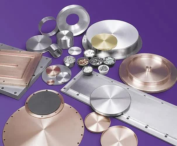
We provide a versatile selection of sputtering targets to meet a wide array of deposition requirements. Our offerings encompass Planar Targets, ideal for standard thin film applications; Rotating Targets, designed to enhance film uniformity and deposition rates; Tubular Targets, suitable for specific coating geometries; and Irregular-shaped Targets, tailored to accommodate unique deposition setups. Our commitment to customization allows us to address specific client needs and application demands effectively. Whether you require standard configurations or have unique preferences, we are dedicated to providing high-quality sputtering targets tailored to your specifications.
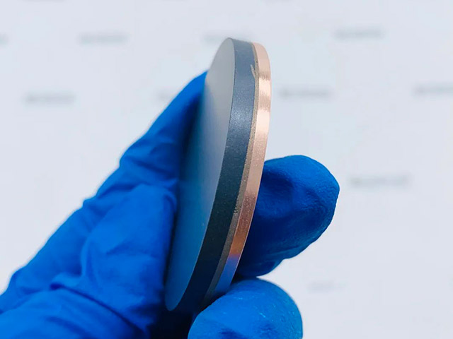
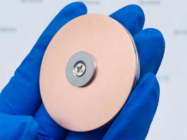
A copper backing plate dissipates heat, preventing deformation or damage to the target during subsequent sputtering. Additionally, it provides mechanical support, electromagnetic shielding, and connectivity, collectively enhancing the efficiency of the sputtering process.
Delivery for small targets is 4-5 weeks. For large targets, the lead time varies based on quantity and material, ranging from 1 to 4 months.
Whether you are exploring the possibility of importing sputtering targets for your project or looking for wholesale distribution opportunities in your local market, we encourage you to contact us. Please contact us for a product that matches your business needs.
If you have other questions about sputtering targets. Please contact us directly, we will answer you with our professional knowledge and experience!
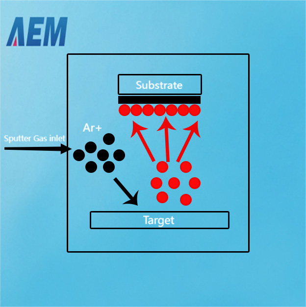
Sputtering target material is a crucial raw material used in the process of manufacturing thin films through Physical Vapor Deposition (PVD). In this process, a high-speed ion beam bombards the solid surface, causing atoms to leave the solid and form a thin film. Sputtering targets find primary applications in various fields such as integrated circuits, semiconductor displays, semiconductor chips, photovoltaic solar energy industries, storage devices, low-emissivity glass in the building/automotive glass industry, decorative coating, and more.
Sputter coating refers to a technique where ions generated by an ion source are accelerated and gathered in a high-speed ion beam in a vacuum. This beam then bombards the solid surface, leading to kinetic energy exchange between ions and surface atoms. This process causes surface atoms to leave the solid and deposit onto the substrate material. The solid being bombarded is the raw material for depositing film using the sputtering method and is known as the sputtering target material. Generally, sputtering targets consist of target blanks and backing plates (or backing tubes). Among these, the target blank is the target material for high-speed ion beam bombardment, making it the core component of sputtering target materials. During the sputtering coating process, after being impacted by ions, atoms on the surface of the target blank are sputtered and deposited on the substrate, forming the thin film material.
As the sputtering target material needs to be installed in specialized equipment for the sputtering process, which involves a high-voltage, high-vacuum working environment, most target blanks are either soft or highly brittle, making them unsuitable for direct installation. Therefore, they need to be bound with backing plates (or backing tubes). The primary function of the backing plates (or backing tubes) is to fix the sputtering target material in place, providing good electrical and thermal conductivity.
The basic principles of sputter coating are illustrated in the following diagram:
Sputter coating technology exhibits excellent repeatability, controllable film thickness, and the ability to achieve uniform thin films on large-area substrates. The prepared films possess high purity, good density, and strong adhesion to the substrate, making sputter coating a primary technique for thin film fabrication. Various types of sputter coating materials have been widely applied, with sputtering targets being among the most extensively used materials in the PVD coating market. Based on different classification methods, sputtering targets can be categorized into several groups.
| Shape |
Planar targets
Rotating targets
Tubular targets
Irregular-shaped targets
|
|---|---|
| Metal Material |
Pure metal targets
Alloy targets
Ceramic targets
Compound targets (oxides, silicides, carbides, etc.)
|
| Application Field |
Targets for flat panel displays
Targets for semiconductor integrated circuits
Targets for solar cell panels
Targets for optical components
Targets for magneto-optical recording media
Targets for automotive coating glass
Targets for research purposes
Targets for tool coating
|
These classifications provide a systematic framework for understanding the diverse applications and types of sputtering targets, enabling tailored solutions for specific coating requirements in various industries.
Sputtering targets are crucial raw materials employed in the fabrication of films using Physical Vapor Deposition (PVD) technology. In this process, high-speed ion beams bombard the solid surface, causing atoms to leave the material and form thin films. This technology finds primary applications in various fields, including integrated circuits, semiconductor displays, semiconductor chips, photovoltaic solar energy, storage devices, low-emissivity glass in the building/automotive glass industry, and decorative coatings.
Modern architecture often incorporates extensive glass facades, providing brighter spaces and expansive views. While this enhances the aesthetic appeal, the increased use of glass in buildings raises concerns about elevated energy consumption due to the transfer of heat through the glass, especially when compared to surrounding walls. Over the past few decades, Low-E (Low Emissivity) coated glass has gained widespread use in the field of architecture.

Low-E glass, also known as low emissivity glass, is a product featuring multiple layers of metal or other compound coatings on the glass surface. The coating layers exhibit characteristics of high transmittance for visible light and high reflectance for mid-to-far infrared radiation. This imparts superior thermal insulation and excellent transparency compared to regular glass and traditional coated glass used in construction.
Architectural Glass:
Easy-to-clean glass (coating imparts hydrophobic properties to the glass surface).
Electrochromic windows (stacked electrochromic layer, responsive to light intensity).
Photovoltaic windows (generate electricity through glass windows).
These applications showcase the versatility of sputtering targets in contributing to advanced functionalities in architectural and automotive glass, addressing concerns related to energy efficiency and environmental sustainability.

Automotive Glass:
Hydrophobic Windshields:Hydrophobic windshields are designed to repel water, enhancing visibility and safety during adverse weather conditions.
Sunlight Control Glass:Sunlight control glass is employed to isolate and protect against high temperatures and ultraviolet damage from the external environment, contributing to enhanced comfort within vehicles.
Anti-Reflection Glass:Anti-reflection glass reduces glare on the dashboard, improving driving visibility and safety.
Materials: Ag (Silver), Al (Aluminum), AZO (Aluminum-doped Zinc Oxide), C (Graphite), Cr (Chromium), Cu (Copper), ITO (Tin-doped Indium Oxide), ZnO (Zinc Oxide), Li (Lithium), Nb (Niobium), NiCr (Nickel Chromium), Si (Pure Silicon), SiAl (Silicon Aluminum), Sn (Tin), SS (Stainless Steel), Ti (Titanium), TiOx (Titanium Oxide), TiOxNb (Niobium Dioxide), T (Tungsten), Zn (Zinc), ZnAl (Zinc Aluminum), ZnSn (Zinc Tin).

The flat-panel display industry is a major application area for high-purity sputtering targets. Flat-panel displays include Liquid Crystal Displays (LCD), Plasma Displays (PDP), Organic Light-Emitting Diode Displays (OLED), and touch panel (TP) display products developed based on LCD. Coating is a fundamental step in the modern flat-panel display industry, and almost all types of flat-panel display devices utilize a significant amount of coating materials to form various functional films. The primary PVD coating materials used are sputtering targets.
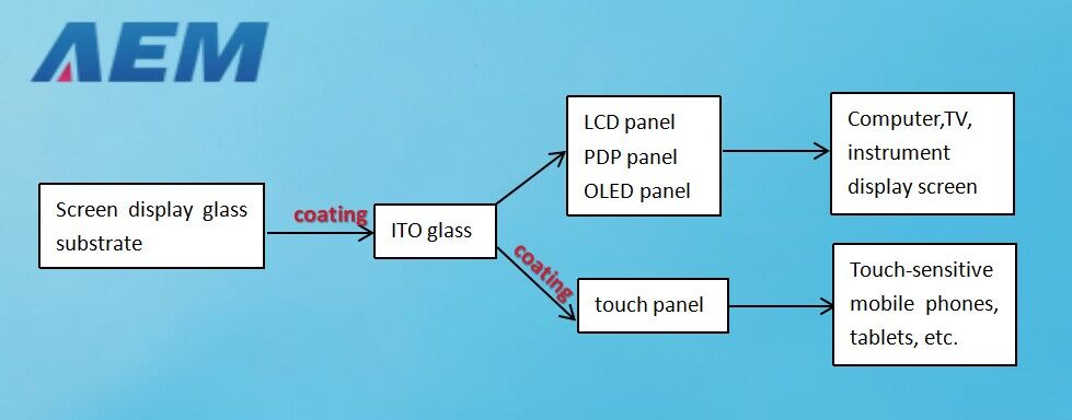
In the production process of flat-panel display panels, the display glass substrate undergoes multiple sputter coating steps to form ITO glass. Subsequently, it undergoes further coating and processing for the production of LCD panels, PDP panels, OLED panels, etc. For touch screens, additional processing is required to form electrodes on ITO glass, followed by assembly with protective screens and other components. To achieve functions such as anti-reflection and anti-glare in flat-panel display products, corresponding film layers can be added during the coating process.

The fabrication of semiconductor chips involves three main stages: silicon wafer manufacturing, wafer fabrication, and chip packaging. In both the wafer fabrication and chip packaging stages, high-purity metal sputtering targets are crucially required.
The types of metal sputtering targets used in the semiconductor chip industry include high-purity targets such as copper, tantalum, aluminum, titanium, cobalt, and tungsten, as well as alloy targets like nickel-platinum, tungsten-titanium, among others.
Copper and tantalum targets are commonly used together. With the ongoing trend towards smaller process nodes in wafer manufacturing, the demand for copper as a wiring material is steadily increasing, indicating sustained growth in the demand for copper and tantalum targets.
Aluminum and titanium targets are often used together. In areas requiring technology nodes above 110nm, such as automotive electronic chips, to ensure stability and interference resistance, a significant amount of aluminum and titanium targets are still required.
Flat panel displays represent the largest domain of target material applications, primarily utilized in semiconductor manufacturing for wafer coating and encapsulation.
These displays encompass Liquid Crystal Displays (LCDs), Plasma Display Panels (PDPs), Thin Film Transistor-Liquid Crystal Displays (TFT-LCDs), among others. Typically composed of metal electrodes, transparent conductive layers, insulating layers, and luminescent layers, flat panel displays extensively employ coating materials to ensure uniformity across large surface areas. This approach aims to enhance productivity and reduce costs. Practically all types of flat panel display devices extensively utilize various coating materials to form diverse functional films. The primary materials used for Physical Vapor Deposition (PVD) coatings are sputtering targets. Notably, many performance aspects of flat panel displays, such as resolution and transparency, are closely associated with the properties of sputtered films.
The process of flat panel display fabrication prominently revolves around the pivotal step of sputter coating.
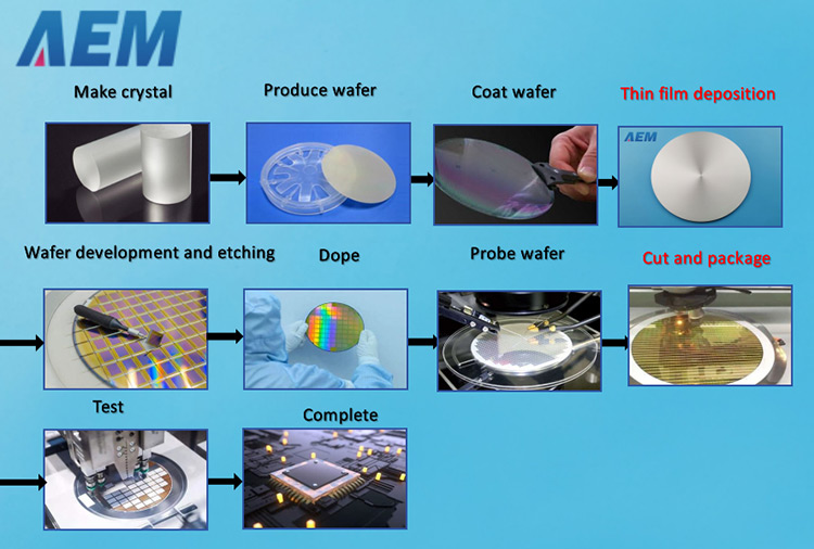
Chips are the soul of mobile phones, representing the pinnacle application domain for sputtering targets. Primarily used in two key stages, 'wafer manufacturing' and 'chip packaging,' these targets typically require a purity level of 5N or higher. Copper, aluminum, molybdenum, and ITO targets are the most commonly and extensively applied.
Advanced processes involving 'copper' and 'tantalum' enable reduced power consumption and enhanced computational speed. 'Aluminum' and 'titanium' processes, above 110nm, ensure reliability and interference resistance in various components such as flash memory chips, processor chips, power management, and sensor chips.
A brief overview of major sputtering targets in the semiconductor field:
Copper targets are applied in conductive layers due to their low electrical resistance, effectively enhancing chip integration. They are extensively used as wiring materials in technology nodes below 110nm.
Aluminum targets are also used in conductive layers, but their limited response speed restricts their usage in technology nodes below 110nm.
Tantalum targets find application in barrier layers, especially high-purity tantalum targets used in high-end semiconductor chips below 90nm on 12-inch wafers, often paired with copper targets.
Titanium targets are similarly applied in barrier layers. High-purity titanium targets are primarily used in technology nodes of 130nm and 180nm on 8-inch wafers, commonly paired with aluminum targets. In automotive electronic chips, aluminum and titanium targets are still extensively employ
Nickel-platinum alloy targets and tungsten targets are used in contact layers, forming a thin film on the silicon layer of the chip, facilitating contact.
Tungsten-nitride alloy targets, with low electron migration rates, serve as contact layer materials in the chip's gate circuits.
Tungsten targets are primarily used in the semiconductor chip memory sector.