Brief Introduction of RF Sputtering
views, Updated: 2021-09-24
Traditional DC Sputtering is a cost-effective way of applying metal target coatings that are electrical conductors like gold. However, DC Sputtering is limited when it comes to dielectric target materials, coatings which are non-conducting insulating materials that can take on a polarized charge. Examples of common dielectric coating materials used in the semiconductor industry include Aluminum Oxide, Silicon Oxide, and Tantalum Oxide.
RF (Radio Frequency) Sputtering is the technique involved in alternating the electrical potential of the current in the vacuum environment at radio frequencies to avoid a charge building up on certain types of sputtering target materials. Over time it can result in arcing into the plasma that spews droplets creating quality control issues on the thin-films. It can even lead to the complete cessation of the sputtering of atoms terminating the process.
As with DC Sputtering, RF Sputtering runs an energetic wave through an inert gas in a vacuum chamber, which becomes ionized. The target material or cathode, which is to become the thin-film coating, is bombarded by these high energy ions sputtering off atoms as a fine spray covering the substrate to be coated. RF Magnetron sputtering uses magnets behind the negative cathode to trap electrons over the negatively charged target material, so they are not free to bombard the substrate, allowing for faster deposition rates.
Advantages of RF Sputtering
1. RF plasmas tend to diffuse throughout the entire chamber rather than concentrating around the cathode or target material as with DC Sputtering.
2. RF Sputtering can sustain a plasma throughout the chamber at a lower pressure (1-15 mTorr). The result is fewer ionized gas collisions equaling more efficient line-of-site deposition of the coating material.
3. Using RF Sputtering, the target material is being “cleaned” with each cycle from building up a charge it helps reduce arcing.
4. RF Sputtering also reduces the creation of “Race track erosion” on the surface of the target material. With Magnetron Sputtering, a circular pattern becomes etched into the surface of the target material as a result of the circular magnetic field of the magnetron focusing the charged plasma particles close to the surface of the sputter target. The diameter of the circular pattern is the result of the magnetic field.
5. With RF Sputtering, the race track's width and depth are much less due to the AC nature of the RF discharge with electrons less confined by the magnetic field. The plasma spreads out more, producing a larger, wider, and shallower racetrack. This makes for better, more uniform, and efficient utilization of target coating materials without the deep etching of “Race track erosion”.
6. RF Sputtering has no disappearing anode effect when the substrate to be coated becomes insulated and acquires a charge as with DC Sputtering.
Thin Film Deposition Materials
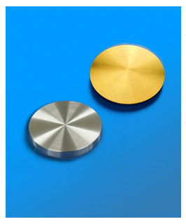
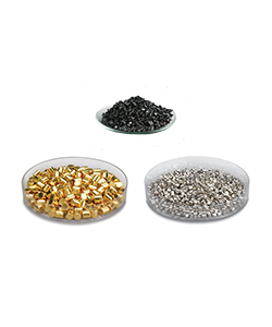
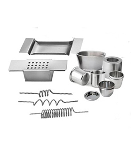
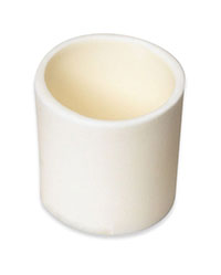
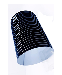
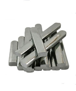
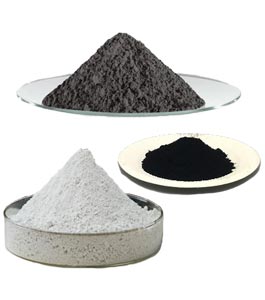
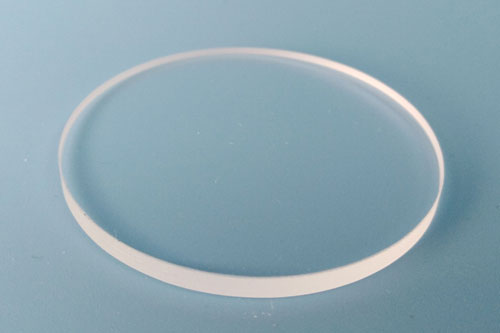
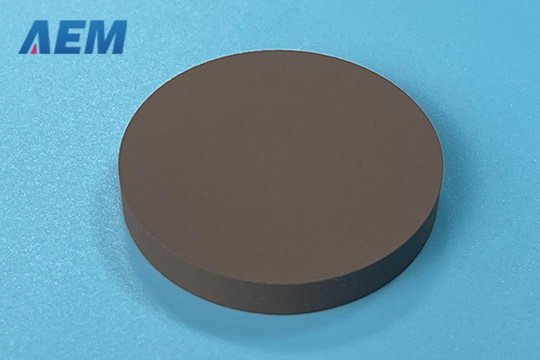
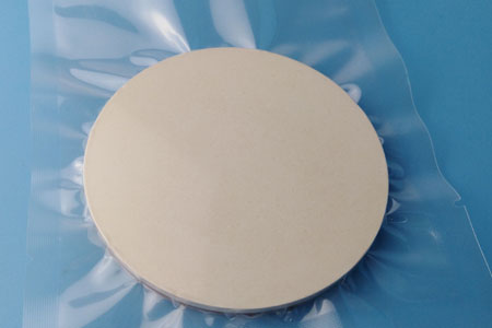
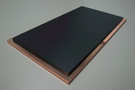
Thin-film deposition materials include but are not limited to sputtering targets and evaporation materials. For more information on types of thin-film coating deposition, please pay sustained attention to AEM Deposition. By the way, AEM Deposition also is an excellent thin-film deposition materials supplier, we provide high-quality sputtering targets (target bonding services also provide), evaporation materials, and other thin-film coating deposition materials.
LATEST NEWS
2024-05-24
2023-10-17
2023-10-17
2023-09-15
2023-09-15
 +86-731-89578196
 [email protected]
