


 +86-731-89578196
 [email protected]

- Home
- Our Company
-
Products
Sputtering Targets
- Industries
- Blog
- FAQ
- Contact Us
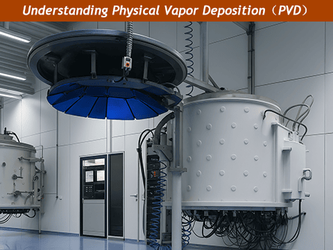
Understanding Physical Vapor Deposition: The Key to Advanced Coatings
1. Introduction to Physical Vapor Deposition (PVD)
In today's world, nearly every industry relies on advanced coatings to improve the durability, performance, and appearance of materials. From the scratch-resistant coating on your smartphone screen to the wear-resistant layer on cutting tools, coatings play a crucial role in modern manufacturing. One of the most widely used and effective coating methods is Physical Vapor Deposition (PVD).
But what exactly is PVD, and why is it so important? Let's break it down in a simple and engaging way.
What is PVD? A Simple Explanation
Physical Vapor Deposition, or PVD, is a high-tech process that applies thin, strong coatings onto various materials. Unlike traditional coating techniques like painting or electroplating, which involve liquids or chemicals, PVD is a dry, vacuum-based process that physically transforms solid materials into a vapor and then condenses them into a thin film on a target surface.
Think of it like this: imagine taking a block of metal, turning it into a fine mist inside a controlled vacuum environment, and then allowing that mist to settle onto another object as an ultra-thin, uniform layer. That's essentially how PVD works—except instead of mist, we're dealing with vaporized atoms!
Why is PVD Important?
PVD plays a crucial role in many high-performance industries because it offers unique benefits that other coating methods cannot match. It is widely used in semiconductors, aerospace, medical devices, automotive parts, optics, and tooling—anywhere that requires durable, high-quality coatings.
Here's why industries choose PVD:
- Extreme Durability: PVD coatings are much harder and more wear-resistant than traditional coatings, making tools and parts last longer.
- Eco-Friendly: Unlike electroplating, which involves harmful chemicals, PVD is a clean and environmentally friendly process.
- High Precision: The coatings are ultra-thin and uniform, ensuring high performance without altering the shape of delicate parts.
- Versatile Material Choices: PVD can be used to coat materials with metals, ceramics, and even specialized alloys, providing endless possibilities for customization.
Where Can You Find PVD in Everyday Life?
You may not realize it, but PVD coatings are all around us! Here are some common examples:
- The gold-colored drill bits at your local hardware store? That's a titanium nitride (TiN) PVD coating, making them harder and more durable.
- The reflective layer on your sunglasses? That's a thin PVD coating that controls light reflection and improves durability.
- The scratch-resistant layer on luxury watches and jewelry? PVD coatings enhance both aesthetics and longevity.
- The protective coatings on medical implants? PVD ensures biocompatibility and long-lasting performance inside the human body.
The Growing Demand for PVD
As industries demand better, longer-lasting, and more environmentally friendly coatings, PVD technology is becoming the gold standard. It provides a superior alternative to traditional coating techniques like electroplating and chemical vapor deposition (CVD).With rapid advancements in manufacturing, the future of PVD is exciting. Engineers and manufacturers continue to explore new materials and processes to make coatings even more durable, efficient, and sustainable.
Final Thoughts
PVD is more than just a coating process—it's a game-changer for modern manufacturing. Whether you're using cutting tools, driving a car, working with electronics, or even wearing sunglasses, chances are you’re benefiting from a PVD coating. In the next sections, we'll dive deeper into how PVD works, the different techniques involved, and how AEM Deposition's high-quality sputtering targets play a vital role in making PVD coatings possible. Stay tuned!
2. How Physical Vapor Deposition Works
Now that we know what Physical Vapor Deposition (PVD) is and why it's important, let's dive deeper into how the process actually works. If you’ve ever wondered how materials like titanium, gold, or even advanced ceramics get transformed into ultra-thin, durable coatings, this section will make it easy to understand.
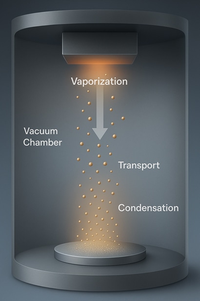
At its core, PVD is a three-step process:
- Vaporization – The coating material (also known as the "source" or "target") is turned into a vapor inside a vacuum chamber.
- Transport – The vaporized material moves through the chamber, unaffected by air or contaminants.
- Condensation – The vaporized atoms settle onto a target surface, forming a strong, uniform thin film.
Let’s break this down further and explore the different ways PVD achieves this.
Step 1: Vaporization – Turning Solids into Vapor
The first and most critical step in PVD is converting the solid coating material into a vapor. This happens inside a vacuum chamber to prevent unwanted reactions with air (like oxidation) and to ensure the material deposits evenly on the target.
There are several ways to vaporize the material, each with its own advantages:
Sputtering – The Most Common PVD Method
Sputtering is one of the most widely used PVD techniques, particularly in electronics, optics, and tool coatings. It works a bit like a microscopic game of billiards!
- A high-energy gas (usually argon) is introduced into the vacuum chamber.
- The gas is electrically charged to form a plasma—a hot, ionized gas that carries energy.
- The plasma’s energetic ions are aimed at the sputtering target (a solid plate of the coating material).
- When the ions hit the target, they knock atoms loose in a controlled manner, turning the solid material into a fine vapor.
- These vaporized atoms then move toward the surface being coated, where they settle into a thin, even layer.
Why is sputtering so popular?
- Precision & Control: The coating thickness can be controlled down to nanometers, making it ideal for microelectronics and optics.
- Versatility: Almost any material—metals, ceramics, alloys—can be sputtered.
- Durability: The coatings are strong, smooth, and adhere well to the substrate.
Real-World Example: How Sputtering is Used
Ever wondered how your smartphone screen stays scratch-resistant? Many screens are coated with a thin indium tin oxide (ITO) layer via sputtering. This transparent, conductive film allows touchscreens to function while protecting them from wear and tear.
Electron Beam Evaporation – Using High Energy to Vaporize Materials
Another method used in PVD is electron beam evaporation, often used for high-purity coatings.
- A strong electron beam (basically a focused stream of energy) is aimed at the material.
- The beam heats the material until it turns into vapor inside the vacuum chamber.
- The vapor rises and condenses onto the target surface, forming a uniform coating.
Why use electron beam evaporation?
- Great for high-melting-point materials like tungsten or platinum.
- Produces extremely pure coatings with minimal contamination.
Real-World Example: High-Performance Optics
High-end telescope lenses and camera filters often use PVD coatings applied via electron beam evaporation. These coatings help control light reflection, enhance clarity, and improve durability.
Thermal Evaporation – The Simpler Approach
In thermal evaporation, the coating material is heated in a crucible or filament until it evaporates and forms a vapor cloud. This vapor then condenses on the target surface.
Why use thermal evaporation?
- Simple and cost-effective – Ideal for thin decorative coatings (e.g., gold-plated jewelry).
- Best for low-melting-point materials like aluminum or magnesium.
Real-World Example: Luxury Watches & Jewelry
The gold-colored coating on high-end watches is often applied using thermal evaporation in a PVD chamber. This provides a durable, scratch-resistant finish without using real gold plating (which can wear off quickly).
Step 2: Transport – Moving the Vapor to the Target
Once the coating material has been vaporized, it needs to travel to the surface it will coat.
- Since the vacuum chamber is free of air, the vaporized atoms move in straight lines without colliding with gas molecules.
- The vapor spreads evenly across the surface, ensuring a uniform coating.
- In some cases, magnetic fields or electric fields are used to further control how the vaporized material moves.
Why is vacuum important?
If PVD were done in a regular atmosphere, oxygen and other gases would react with the vaporized material, causing defects in the coating. That’s why a high vacuum (low-pressure) environment is crucial for high-quality coatings.
Step 3: Condensation – Forming the Thin Film
After the vaporized material reaches the target surface, it settles and bonds, forming an ultra-thin, durable coating.
- The deposited film builds up atom by atom, ensuring strong adhesion.
- The coating can be as thin as a few nanometers (for high-precision applications) or several micrometers (for wear-resistant coatings).
- By adjusting temperature, gas composition, and deposition rate, manufacturers can fine-tune the coating’s hardness, conductivity, reflectivity, and other properties.
How Long Does PVD Coating Take?
- A thin, decorative PVD coating (like on a watch) can take a few minutes.
- A high-performance industrial coating (like for aerospace parts) may require several hours for optimal thickness.
Final Thoughts: The Role of AEM Deposition in PVD
A crucial part of the PVD process is the material being deposited—which comes from high-quality sputtering targets or evaporation materials.
As a leading sputtering target supplier, AEM Deposition specializes in producing premium-quality sputtering targets and PVD materials for industries worldwide. Whether you require pure metal, alloy, or ceramic targets, our solutions deliver consistent, high-performance coatings tailored to your applications.
3. Key Applications of PVD in Industry

1. Semiconductor & Electronics
-
Microchips & Circuit Boards – PVD is used to deposit conductive metal layers (like aluminum, copper, and gold) on semiconductor wafers. These coatings form the tiny connections that make your phone, computer, and other devices function. -
Touchscreens & Displays – Transparent conductive coatings (such as Indium Tin Oxide, or ITO) are applied via PVD to allow touchscreens to respond accurately while staying durable.
2. Aerospace & Automotive
In high-performance industries like aerospace and automotive, durability is everything. PVD coatings help critical components withstand extreme conditions.
- Jet Engine Parts & Turbines – PVD coatings protect against heat, corrosion, and wear, ensuring these high-stress components last longer.
- Car Engine Parts – Automotive companies use PVD to coat pistons, gears, and valves, reducing friction and extending engine life.
- Decorative Finishes – PVD provides scratch-resistant, metallic finishes on car parts and trim without the environmental drawbacks of chrome plating.
Real-World Example: Many modern cars feature PVD-coated parts to improve engine efficiency and fuel economy.
3. Medical Devices & Implants
The medical field requires biocompatible, sterile, and wear-resistant coatings—all of which PVD provides.
- Surgical Tools – Scalpels, forceps, and other surgical instruments are PVD-coated for longer lifespan, resistance to sterilization, and reduced friction during procedures.
- Medical Implants – Artificial joints, stents, and dental implants use PVD coatings (like Titanium Nitride, TiN) to improve biocompatibility and prevent wear inside the human body.
Real-World Example: Hip replacements and heart stents often have PVD coatings to prevent reactions with body tissues.
4. Optics & Solar Panels
PVD coatings enhance optical components by controlling light reflection, glare, and durability.
- Lenses & Glasses – Anti-reflective and scratch-resistant coatings applied via PVD make eyeglasses, camera lenses, and telescopes clearer and longer-lasting.
- Solar Panels – Thin films of silicon, silver, and other metals are deposited on solar cells to improve energy absorption and efficiency.
Real-World Example: The anti-glare coating on your sunglasses is most likely applied using PVD.
5. Tooling & Industrial Equipment
Industrial tools take a beating, but PVD coatings make them last much longer.
- Cutting Tools & Drills – Coatings like Titanium Nitride (TiN) and Chromium Nitride (CrN) increase hardness, reduce wear, and improve cutting performance.
- Molds & Dies – PVD protects manufacturing molds from friction and heat, helping them produce more parts before needing replacement.
Real-World Example: Those gold-colored drill bits at the hardware store? That’s a PVD Titanium Nitride coating making them harder and more durable.
Final Thoughts: Why PVD is Everywhere
PVD technology is transforming industries by extending the life of products, improving performance, and reducing environmental impact. Whether in electronics, aerospace, medical devices, optics, or industrial tools, PVD coatings make everyday products stronger, more efficient, and more reliable.
In the next section, we’ll explore why PVD is a better choice compared to other coating methods—and how AEM Deposition’s high-quality sputtering targets play a key role in this process. Stay tuned!
4. Advantages of Physical Vapor Deposition (PVD)
Now that we’ve seen where Physical Vapor Deposition (PVD) is used, let’s talk about why manufacturers, engineers, and researchers prefer PVD over other coating techniques. The short answer? It’s cleaner, stronger, and more precise.
PVD coatings offer several key advantages, making them ideal for industries that require high-performance, long-lasting coatings. Below, we’ll explore the main benefits that set PVD apart from other coating methods.
1. Superior Durability & Hardness
One of the biggest reasons industries choose PVD is its extreme hardness and wear resistance.
- PVD coatings create a surface that is much harder than the base material, making tools and components last significantly longer.
- These coatings resist scratches, corrosion, and high temperatures, maintaining performance even in harsh environments.
- Unlike traditional plating (like electroplating), PVD coatings don’t chip, peel, or wear away easily.
Real-World Example: Cutting tools like drill bits, saw blades, and end mills last 3 to 5 times longer with a PVD coating because it reduces wear and friction.
Why it matters: In industrial applications, longer-lasting tools mean less downtime, fewer replacements, and lower costs.
2. Environmentally Friendly (No Toxic Chemicals!)
Many traditional coating processes—such as electroplating and chemical vapor deposition (CVD)—use harmful chemicals, acids, or gases that generate hazardous waste. PVD, on the other hand, is an eco-friendly process that eliminates these concerns.
- No toxic byproducts – PVD doesn’t require harsh chemicals like cyanides, hexavalent chromium, or acids used in electroplating.
- No hazardous waste – Unlike electroplating, which produces chemical waste, PVD is a clean, vacuum-based process with minimal environmental impact.
- Safer for workers & the planet – Since PVD is a dry process, there’s no risk of chemical exposure for workers, making it a safer choice for manufacturers.
Real-World Example: Many automotive companies are switching from chrome electroplating (which is toxic) to PVD coatings for car trims, reducing environmental pollution.
Why it matters: Manufacturers can meet strict environmental regulations while improving product quality.
3. High Precision & Uniformity
PVD allows engineers to precisely control coating thickness down to the nanometer level, making it ideal for advanced applications.
- Uniform coatings – The vacuum-based deposition ensures a perfectly even layer, free from defects or inconsistencies.
- Atomic-level precision – PVD can create layers as thin as a few nanometers, critical for electronics, optics, and aerospace.
- Controlled film properties – Engineers can fine-tune the hardness, reflectivity, conductivity, and even color of the coating.
Real-World Example: Semiconductor manufacturers rely on PVD to deposit ultra-thin metal layers (such as copper and aluminum) on microchips, ensuring high-speed data transfer.
Why it matters: In industries like electronics and optics, even the smallest imperfections can cause failures, so PVD’s precision is crucial.
4. Strong Adhesion – No Peeling or Flaking
Unlike painted or plated coatings, PVD forms a direct atomic bond with the substrate, ensuring superior adhesion.
- The coating becomes part of the surface instead of just sitting on top, preventing peeling or flaking.
- Even under high stress, PVD coatings stay intact, making them perfect for tools, medical implants, and aerospace components.
Real-World Example: High-speed machining tools, coated with Titanium Aluminum Nitride (TiAlN) via PVD, maintain their coating even after intense heat and friction.
Why it matters: Better adhesion means longer-lasting performance with less risk of failure.
5. Heat & Corrosion Resistance
PVD coatings provide exceptional resistance to extreme temperatures, oxidation, and chemical corrosion, making them ideal for harsh environments.
- Many PVD coatings can withstand temperatures above 1000°C without breaking down.
- PVD coatings protect against moisture, chemicals, and oxidation, extending the lifespan of parts.
- Even under thermal cycling (heating and cooling repeatedly), PVD coatings remain stable.
Real-World Example: Aerospace turbine blades are PVD-coated with ceramic or nitride layers to withstand the intense heat of jet engines.
Why it matters: In industries like aerospace and medical, corrosion resistance ensures safety and long-term reliability.
6. Customizable Aesthetics – Color & Finish Control
While PVD is often used for functional coatings, it’s also a popular choice for decorative applications.
- PVD coatings can be matte, glossy, or metallic in appearance.
- Engineers can deposit colored coatings (like gold, black, blue, or rainbow finishes) by adjusting the process parameters.
- Unlike traditional coatings, PVD finishes don’t fade, tarnish, or wear off easily.
Real-World Example: Many luxury watch brands use gold PVD coatings instead of real gold plating for a scratch-resistant, long-lasting finish.
Why it matters: PVD coatings look great while staying durable, making them ideal for jewelry, watches, and high-end consumer products.
Final Thoughts: Why More Industries are Choosing PVD
With superior durability, eco-friendly processing, and high-precision application, it’s no surprise that PVD is quickly replacing older coating technologies. Whether it’s cutting tools, aerospace components, electronics, medical devices, or luxury goods, PVD coatings offer unmatched performance, longevity, and reliability.
At AEM Deposition, we specialize in supplying high-quality sputtering targets for PVD applications. Our materials help manufacturers achieve stronger, more precise, and longer-lasting coatings for industries worldwide.
In the next section, we’ll compare PVD with other deposition techniques like CVD, electroplating, and thermal spray coatings to see why PVD is often the better choice. Stay tuned!
5. Comparison of PVD with Other Deposition Techniques
Now that we’ve covered the advantages and challenges of Physical Vapor Deposition (PVD), it’s time to see how it compares to other popular coating methods. While PVD is an advanced technology, it’s not the only option—manufacturers also use Chemical Vapor Deposition (CVD), Electroplating, and Thermal Spray Coatings depending on their needs.
So, how does PVD stack up? Let’s break it down.
1. PVD vs. Chemical Vapor Deposition (CVD)
Both PVD and CVD are vacuum-based thin-film deposition techniques, but they work differently.
|
Feature |
PVD (Physical Vapor Deposition) |
CVD (Chemical Vapor Deposition) |
|
Process Type |
Physical (material is vaporized and condensed) |
Chemical (gas-phase reactions form a coating) |
|
Temperature Required |
Low to medium (200°C – 500°C) |
High (600°C – 1000°C) |
|
Coating Purity |
High purity with minimal contamination |
Can introduce impurities from chemical reactions |
|
Coating Thickness |
Typically 0.1 – 5 microns |
Can be thicker (1 – 50 microns) |
|
Geometric Coverage |
Line-of-sight (can struggle with complex shapes) |
Conformal (better for coating complex 3D parts) |
|
Environmental Impact |
No harmful byproducts |
Uses toxic gases, requires waste management |
When to Choose PVD vs. CVD?
- Use PVD when you need:Hard, wear-resistant coatings (e.g., cutting tools, optics, electronic films) with high purity.
- Use CVD when you need:Thicker coatings and full 3D coverage (e.g., diffusion barriers in semiconductors, protective coatings on turbine blades).
Example: In semiconductor manufacturing, PVD is used for metal coatings (like aluminum or copper interconnects), while CVD is preferred for insulating layers (such as silicon dioxide coatings).
2. PVD vs. Electroplating
Electroplating is one of the oldest and most widely used coating processes, but it differs significantly from PVD.
|
Feature |
PVD |
Electroplating |
|
Process Type |
Vacuum-based physical deposition |
Liquid-based chemical deposition |
|
Adhesion |
Strong atomic bonding |
Can peel or flake over time |
|
Hardness |
Very hard coatings (e.g., TiN, CrN) |
Softer metal coatings (e.g., gold, nickel) |
|
Environmental Impact |
Eco-friendly (no toxic chemicals) |
Produces hazardous waste (heavy metals, acids) |
|
Material Versatility |
Works with metals, ceramics, and alloys |
Mostly used for metals (gold, nickel, chrome) |
|
Coating Thickness |
Thin (0.1 – 5 microns) |
Can be much thicker (5 – 500 microns) |
When to Choose PVD vs. Electroplating?
- Use PVD when you need:High-performance coatings with superior wear resistance (e.g., cutting tools, medical implants).
- Use Electroplating when you need:Thicker metallic coatings for decorative or corrosion-resistant purposes (e.g., jewelry, automotive chrome plating).
Example: Many luxury watch brands are switching from electroplating to PVD gold coatings because PVD lasts longer and doesn’t fade over time.
3. PVD vs. Thermal Spray Coatings
Thermal spray coatings (including plasma spraying and High-Velocity Oxy-Fuel (HVOF) spraying) are widely used for thick, protective coatings on large components.
|
Feature |
PVD |
Thermal Spray Coatings |
|
Process Type |
Atomic-level vapor deposition |
Molten or semi-molten material sprayed onto a surface |
|
Coating Thickness |
Thin (0.1 – 5 microns) |
Thick (50 microns – several millimeters) |
|
Surface Finish |
Smooth, uniform |
Rough, textured |
|
Material Options |
Metals, ceramics, nitrides |
Metals, ceramics, carbides |
|
Adhesion |
Excellent (atomic bonding) |
Good but requires rough surface for adhesion |
|
Best For |
Thin, precise, high-performance coatings |
Wear-resistant coatings on large parts |
When to Choose PVD vs. Thermal Spray?
- Use PVD when you need:Thin, high-performance coatings with excellent hardness and precision (e.g., cutting tools, optics, electronics).
- Use Thermal Spray when you need:Thicker coatings for corrosion, heat, or impact resistance (e.g., aircraft turbine blades, industrial rollers).
Example: Aerospace engine parts use both technologies—PVD for thin, heat-resistant coatings and thermal spray for thick protective layers against wear and corrosion.
Final Comparison: Which Deposition Method is Best?
|
Factor |
PVD |
CVD |
Electroplating |
Thermal Spray |
|
Best for Thin Films |
✅ Yes |
✅ Yes |
❌ No |
❌ No |
|
Best for Thick Coatings |
❌ No |
✅ Yes |
✅ Yes |
✅ Yes |
|
High Hardness |
✅ Yes |
✅ Yes |
❌ No |
✅ Yes |
|
Complex Shapes |
❌ Limited |
✅ Yes |
✅ Yes |
❌ Limited |
|
Eco-Friendly |
✅ Yes |
❌ No |
❌ No |
✅ Yes |
|
Wear Resistance |
✅ Yes |
✅ Yes |
❌ No |
✅ Yes |
|
Cost-Effective for Large Volumes |
❌ No |
❌ No |
✅ Yes |
✅ Yes |
Final Thoughts: Why More Industries Are Choosing PVD
While each deposition method has its place, PVD is becoming the go-to choice for manufacturers who need hard, durable, high-purity coatings with minimal environmental impact.
- PVD vs. CVD: PVD is better for low-temperature, high-purity coatings, while CVD excels at thicker, more conformal coatings.
- PVD vs. Electroplating: PVD is stronger, cleaner, and more durable, while electroplating is cheaper for thick metal coatings.
- PVD vs. Thermal Spray: PVD is great for thin, precise coatings, while thermal spray is better for thicker, wear-resistant coatings on large components.
At AEM Deposition, we provide high-quality sputtering targets that help manufacturers achieve top-tier PVD coatings across electronics, aerospace, medical, and industrial applications.
In the next section, we’ll take a closer look at sputtering targets—the key material used in PVD—and why their quality is essential for high-performance coatings. Stay tuned!
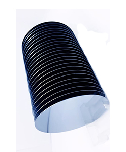
7. The Role of Sputtering Targets in PVD
Now that we’ve seen how PVD compares to other deposition methods, let’s focus on a critical component of the PVD sputtering process—sputtering targets. These targets are the raw materials that get transformed into high-performance coatings in industries like electronics, aerospace, medical devices, and industrial tooling.
In this section, we’ll explore what sputtering targets are, why they matter, and how AEM Deposition provides high-quality materials for the industry.
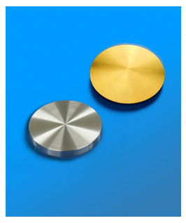
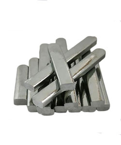
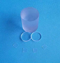
What Are Sputtering Targets?
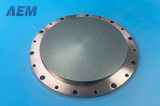
A sputtering target is a solid piece of material (metal, alloy, ceramic, or composite) used in the PVD sputtering process to create thin films. During sputtering, high-energy plasma ions bombard the target, causing its atoms to be ejected and deposited onto a surface as a thin, uniform film.
Think of it like spraying paint onto a wall—but at an atomic level. Instead of using liquid paint, PVD sputtering ejects atoms from a solid target and transfers them onto the desired surface in a controlled vacuum environment.
The quality of the sputtering target directly affects the quality of the thin film, making it a crucial part of the PVD process.
Why Are Sputtering Targets Important?
The purity, composition, and structure of a sputtering target determine how well it performs during deposition. Here’s why choosing high-quality sputtering targets matters:
- Film Purity & Performance – Higher purity targets produce cleaner coatings with fewer defects. This is essential in semiconductors, optical coatings, and medical implants, where even microscopic impurities can cause failures.
- Coating Uniformity – Well-engineered targets improve film thickness control, ensuring even, consistent coatings.
- Deposition Efficiency – Targets with optimized microstructure allow for faster and more efficient sputtering, reducing production time and costs.
- Longer Target Life – High-quality targets wear evenly, leading to stable coating performance over time and less material waste.
- Material Versatility – Sputtering targets can be made from metals, alloys, ceramics, and composites, allowing for a wide range of coating properties (e.g., conductive, reflective, wear-resistant, biocompatible).
Real-World Example:
In semiconductor manufacturing, thin films must be extremely pure and defect-free. A sputtering target with 99.999% purity ensures that the deposited film has minimal contamination, improving the reliability of microchips in smartphones, computers, and advanced electronics.
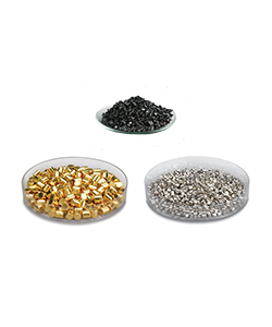
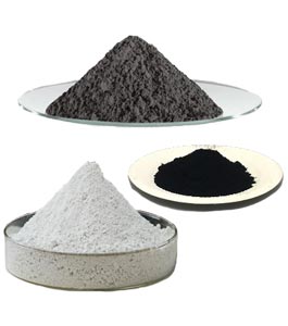
Common Materials Used for Sputtering Targets
Different industries require different sputtering target materials based on the coating’s purpose. Here are some of the most commonly used materials:
1. Metal Sputtering Targets
Aluminum (Al) – Used in microelectronics, touchscreens, and solar panels.
Copper (Cu) – Ideal for semiconductor interconnects, circuit boards, and thermal management coatings.
Titanium (Ti) – Common in medical implants, aerospace, and decorative coatings.
Tantalum (Ta) – Found in capacitors, memory storage devices, and corrosion-resistant coatings.
Example: In smartphone displays, Indium Tin Oxide (ITO) sputtering targets are used to create transparent conductive coatings that allow touchscreens to function.
2. Alloy Sputtering Targets
Titanium-Aluminum (TiAl) – Used for hard coatings in cutting tools and aerospace components.
Nickel-Chromium (NiCr) – Found in resistive films and corrosion-resistant coatings.
Molybdenum-Tungsten (MoW) – Used in thin-film transistors (TFTs) for displays.
3. Ceramic & Oxide Sputtering Targets
Silicon Dioxide (SiO₂) – Used in optical coatings, semiconductor devices, and solar panels.
Zinc Oxide (ZnO) – Applied in transparent conductive films for displays.
Aluminum Oxide (Al₂O₃) – Found in protective coatings for wear resistance and insulation layers.
Example: Optical lenses and camera filters use high-purity SiO₂ sputtering targets to create anti-reflective coatings that improve clarity.
Quality Matters: Choosing the Right Sputtering Targets
The quality of sputtering targets significantly affects the coating outcomes. AEM Deposition supplies high-purity targets to ensure exceptional coating performance, consistency, and efficiency. Our materials are precisely engineered to meet diverse industry demands, from electronics and optics to aerospace and healthcare.
For tailored sputtering targets suited for your precise needs, visit our Sputtering Targets Products.
Final Thoughts
Physical Vapor Deposition is transforming industries with durable, precise, and environmentally responsible coatings. Choosing high-quality sputtering targets and evaporation materials ensures optimal results and competitive advantages.
At AEM Deposition, we deliver the precision, quality, and reliability your industry demands. Ready to enhance your coating performance? Contact our team today to learn more about how we can support your next project.