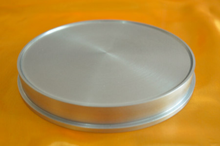
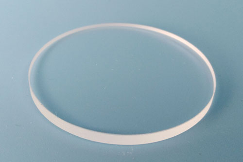
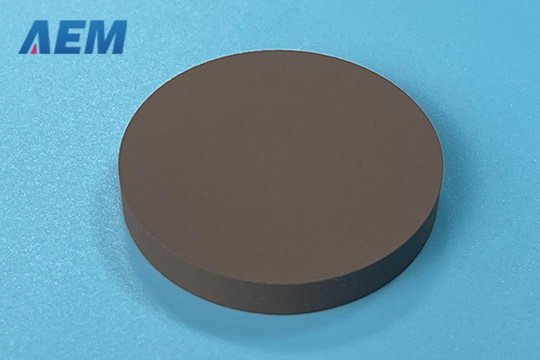
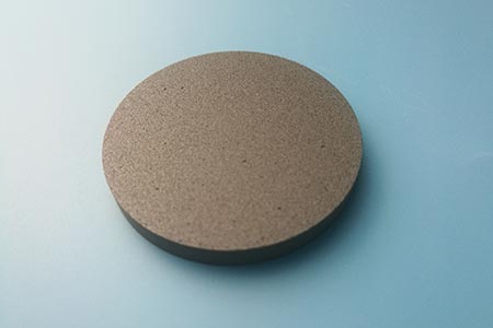
Silicon Sputtering Targets (Si)
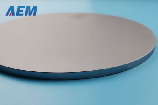

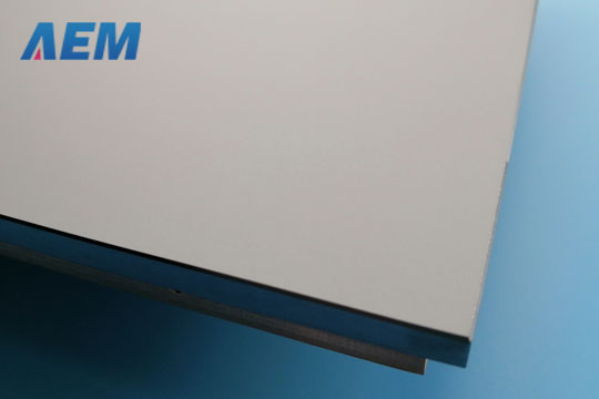
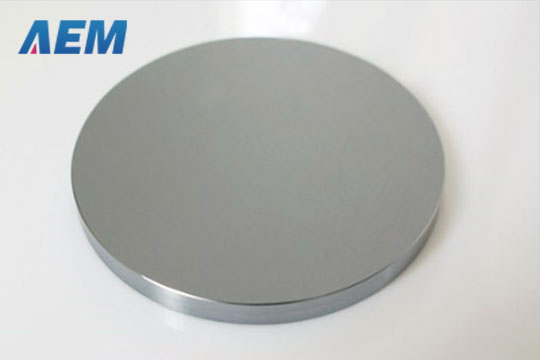
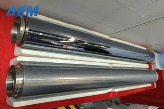
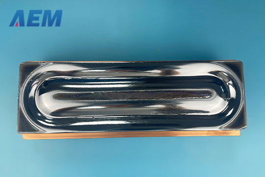
| Material Type | Silicon |
| Symbol | Si |
| Atomic Weight | 28.0855 |
| Atomic Number | 14 |
| Color/Appearance | Dark Gray with a Bluish Tinge, Semi-Metallic |
| Thermal Conductivity | 150 W/m.K |
| Melting Point (°C) | 1,410 |
| Bulk Resistivity | >1 OHM-CM, 0.005-0.020 OHM-CM, <0.1 OHM-CM |
| Coefficient of Thermal Expansion | 2.6 x 10⁻⁶/K |
| Theoretical Density (g/cc) | 2.32 |
| Dopant | Undoped, Boron, Phosphorous, Arsenic, or Antimony |
| Z Ratio | 0.712 |
| Sputter | RF |
|
Max Power Density* (Watts/Square Inch) |
20 |
| Type of Bond | Indium, Elastomer |
| Comments | Alloys with W; use heavy W boat. SiO produced. |
Silicon Sputtering Targets
Silicon is solid at room temperature, melting at 1,414°C (2,577°F) and boiling at 3,265°C (5,909°F). It's unique because it expands when it freezes, like ice. Silicon is great at conducting heat.
Silicon sputtering targets are used in reactive magnetron sputtering to create dielectric layers like SiO2 and SiN. These layers have useful properties, like hardness, clear optics, and the ability to insulate. They also resist wear and corrosion, making them important in things like high-tech glass and microelectronics.
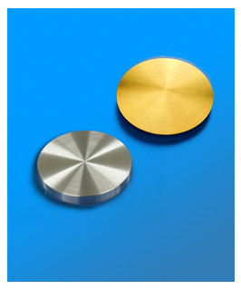
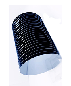
These sputtering targets are used in various applications, including making clear glass for LCD screens, energy-efficient architectural glass, and microelectronics. There are two types: single crystal and polycrystalline. We create flat silicon sputtering targets using a method called Czochralski crystal growth.
Silicon Sputtering Targets Information
Silicon Sputtering Targets
Purity: 99.99%, 99.999%;
Relative density: ≥ 95%;
Conductivity type: P-type & N-type;
Circular: Diameter <= 14 inch, Thickness >= 1mm;
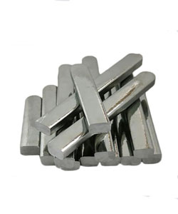
Block: Length <= 32 inch, Width <= 12 inch, Thickness >= 1mm;
Targets type: Planar sputtering target, Rotary sputtering target.
Bonding is recommended for these materials. Many materials have characteristics that are not amenable to sputtering, such as brittleness and low thermal conductivity. This material may require a special ramp up and ramp down procedures. This process may not be necessary for other materials. Targets that have low thermal conductivity are susceptible to thermal shock.
More Information on Silicon Sputtering Targets
Applications• Optical and decoration coating• Semiconductor and thin film solar energy • Flat panel displays |
Features• Competitive pricing• High purity • Grain refined, Engineered microstructure • Semiconductor grade |
Manufacturing Process• RefiningThree-layer electrolytic process • Melting and casting Electrical resistance furnace - Semi-continuous casting • Grain refinement Thermomechanical treatment • Cleaning and final packaging - Cleaned for use in vacuum Protection from environmental contaminants Protection during shipment |
Options• 99.99% minimum purity• Semiconductor grade silicon alloys available Al/Si, Al/Cu/Si • Smaller sizes also available for R&D applications • Sputtering target bonding service |
Related Products of Silicon Sputtering Targets
|
|
Ceramic Sputtering Targets Silicon Dioxide Sputtering Target |
|
|
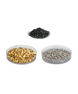
Evaporation Materials Silicon Evaporation Pellet |
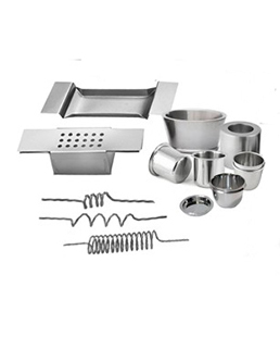
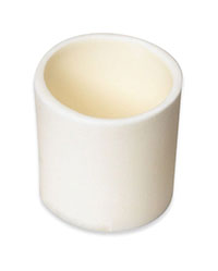
Crucibles Quartz Crucible |
Metal Powders N/A |
 Click to download datasheet about Silicon Sputtering Targets (Si)
 Unable to find the required data sheet? Click here to send an email and get it.
 Click here to get answers to Frequently Asked Questions (FAQ).


