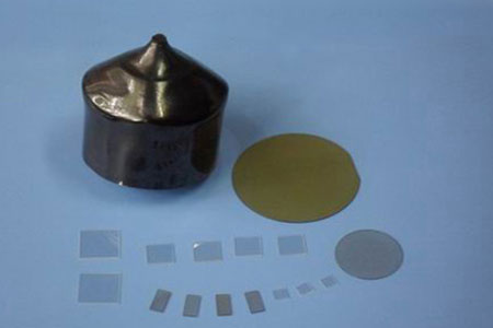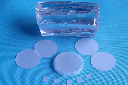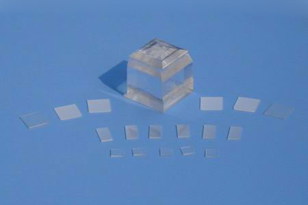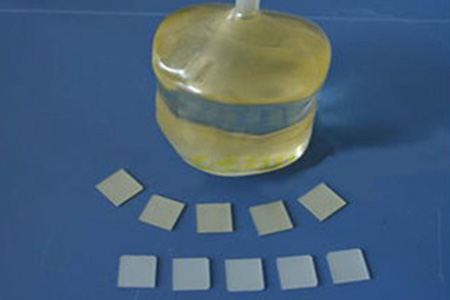
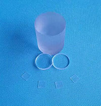
Neodymium Gallate Substrate (NdGaO3)
Neodymium Gallate Substrate
Neodymium Gallate (NdGaO3) is a single crystal substrate mainly used for epitaxial film growth of high-temperature superconductors (such as YBCO) and magnetic materials. It can produce epitaxially film in good quality because the lattice mismatch is small (~0.27%) between NdGaO3 and YBCO, and there is no structural phase transition.
Neodymium Gallate Substrate Physical Properties
| Material | NdGaO3 |
|---|---|
| Structure | Orthor. |
| Lattice (A) | a=5.43, b=5.5, c=7.71 |
| Growth Method | Czochralski |
| Melting Point | 1600℃ |
| Density(g/cm3) | 7.57g/cm3 |
| Permittivity | ε = 25 |
Neodymium Gallate Substrate Specifications
| Size | 10x3, 10x5, 10x10, 15x15, 20x20,Dia 15 mm, Dia 20 mm, Dia 1'', Dia 2'' |
|---|---|
| Thickness | 0.5 mm, 1.0 mm |
| Polished | SSP or DSP |
| Orientation | <100>, <110>, <111> |
| Redirection Precision | ±0.5° |
| Redirection the Edge | 2°(special in 1°) |
| Angle of Crystalline | Special size and orientation are available on demand. |
| Ra: | ≤5Å(5µm×5µm) |
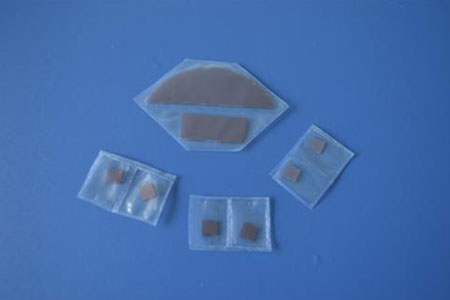
Neodymium Gallate Substrate Package
Packaged with class 100 clean bag or wafer container in a class 1000 clean room.
Related Products of Neodymium Gallate Substrate
|
Magnetic Ferroelectricity Substrates |
Semiconductor Wafers |
|
|
GaN Thin Film Substrates |
Halide Substrates |
Ceramic Substrates |
FREE QUOTE
 Click to download datasheet about Neodymium Gallate Substrate (NdGaO3)
 Unable to find the required data sheet? Click here to send an email and get it.
 Click here to get answers to Frequently Asked Questions (FAQ).