


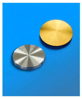
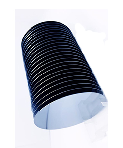
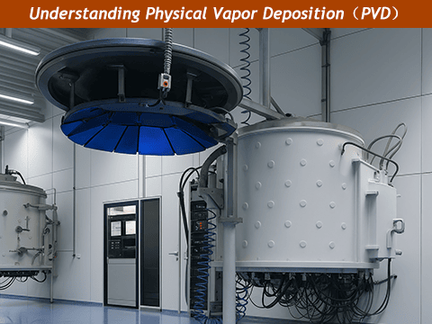
Understanding Physical Vapor Deposition: The Key to Advanced Coatings
Date: 2025-04-09
Abstract: Learn how Physical Vapor Deposition provides durable, precise coatings. Discover benefits, applications, and quality sputtering targets at AEM Deposition.
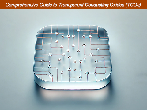
Comprehensive Guide to Transparent Conducting Oxides (TCOs)
Date: 2025-02-28
Abstract: Understanding Transparent Conducting Oxides (TCOs) and how AEM Deposition's sputtering targets deliver superior performance.
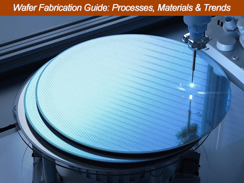
Wafer Fabrication Guide: Processes, Materials & Trends in 2025
Date: 2025-01-24
Abstract: Discover the wafer fabrication process, from material prep to advanced production. Stay ahead with AEM Deposition's premium wafers and cutting-edge trends.
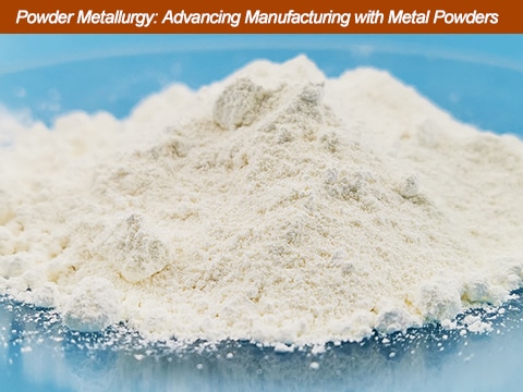
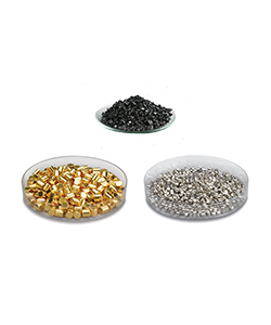
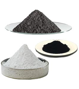
Powder Metallurgy: Advancing Manufacturing Processes with High-Quality Spherical Metal Powders
Date: 2025-01-10
Abstract: Discover how spherical powders are revolutionizing powder metallurgy, creating stronger, more precise, and higher-performing parts. Learn more!
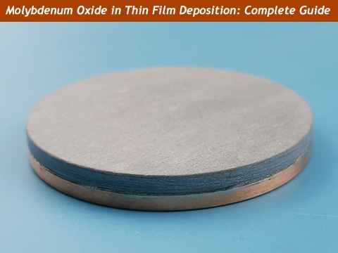
Molybdenum Oxide in Thin Film Deposition: Benefits, Applications, and Comparisons
Date: 2024-12-27
Abstract: Explore the role of molybdenum oxide (MoO₃) in thin film deposition, its benefits, applications, and how it compares to other materials.
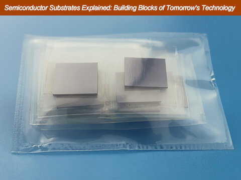
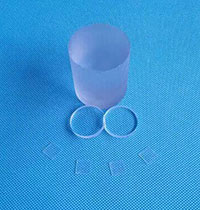
Semiconductor Substrates Explained: Building Blocks of Tomorrow's Technology
Date: 2024-09-14
Abstract: Boost your technology with our semiconductor substrates designed for precision and reliability. Contact us today for your custom solutions.
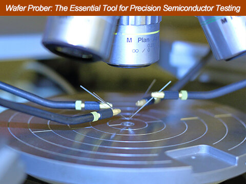
Wafer Prober: The Essential Tool for Precision Semiconductor Testing
Date: 2024-09-10
Abstract: Learn all about wafer probers and how they improve semiconductor testing precision, efficiency, and production yield. Explore our expert insights today.
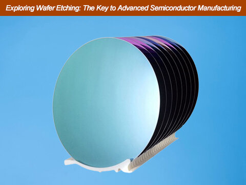
Exploring Wafer Etching: The Key to Advanced Semiconductor Manufacturing
Date: 2024-07-30
Abstract: Explore various wafer etching processes that ensure superior semiconductor quality. Get high-quality wafers and substrates from us. Reach out now!
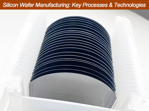
Silicon Wafer Manufacturing: Key Processes & Technologies
Date: 2024-06-07
Abstract: Discover the essential steps and technologies in silicon wafer manufacturing, enhancing wafer quality, and developing electronics.
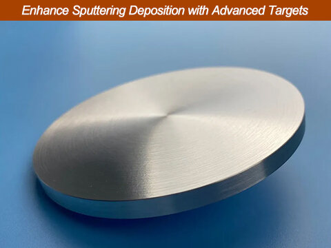
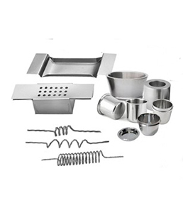
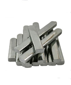
Enhance Your Sputtering Deposition Performance with Cutting-Edge Sputtering Targets
Date: 2024-07-01
Abstract: Discover how sputtering deposition and premium sputtering targets enhance coating quality. Learn about their importance, basics, and future trends.
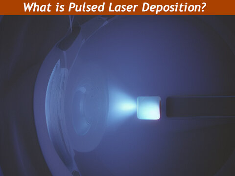
What is Pulsed Laser Deposition: An In-Depth Exploration
Date: 2023-09-15
Abstract: Discover the world of Pulsed Laser Deposition (PLD) and its role in material science. Such as what is PLD and why is it special.
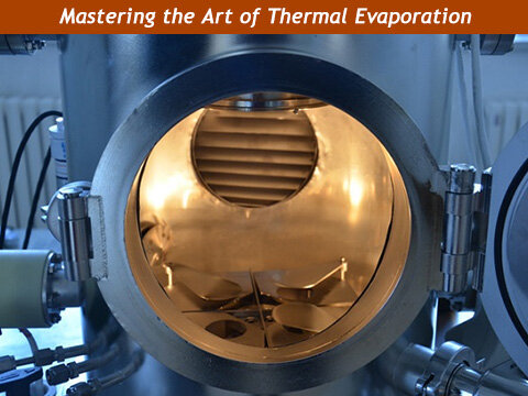
The Art of Thermal Evaporation: A Step-by-Step Guide
Date: 2023-09-15
Abstract: Learn about thermal evaporation in this comprehensive guide. Explore the principles, step-by-step process, and various industry applications of this technique.